Time: 2025-03-03 11:56:47View:
The FPGA (Field-Programmable Gate Array) development process involves several stages, from design conception to final implementation (burning the configuration onto the FPGA). Below is a detailed explanation of each step in the FPGA development process:
Objective: Define the functionality and requirements of the system.
Tasks:
Identify the problem to be solved.
Specify input/output interfaces, performance requirements, and constraints (e.g., power, area, speed).
Create a high-level block diagram of the system.
Output: A detailed design specification document.
Objective: Create a hardware description of the system.
Methods:
Use tools like Xilinx Vivado HLS or Intel HLS Compiler to generate HDL code from high-level languages like C/C++.
Use graphical tools to create a design by connecting pre-defined logic blocks.
Use languages like VHDL or Verilog to describe the behavior and structure of the design.
Example: Writing modules for specific functions (e.g., counters, state machines).
Hardware Description Languages (HDLs):
Schematic Entry:
High-Level Synthesis (HLS):
Output: HDL code or schematic files.
Objective: Verify the correctness of the design before synthesis.
Tasks:
Write testbenches in HDL to simulate the design.
Use simulation tools like ModelSim, Vivado Simulator, or QuestaSim.
Test for functional correctness, edge cases, and timing behavior.
Output: Simulation results (waveforms, logs) confirming the design works as expected.
Objective: Convert the HDL design into a gate-level netlist.
Tasks:
Use synthesis tools like Xilinx Vivado, Intel Quartus, or Synopsys Design Compiler.
Map the HDL code to the FPGA's primitive logic elements (LUTs, flip-flops, DSP blocks, etc.).
Optimize for area, speed, and power.
Output: A gate-level netlist (e.g., EDIF file).
Objective: Map the synthesized netlist onto the physical resources of the FPGA.
Tasks:
Placement: Assign logic elements to specific locations on the FPGA.
Routing: Connect the placed elements using the FPGA's routing resources.
Optimize for timing, power, and resource utilization.
Output: A configuration file (bitstream) that defines the FPGA's internal connections.
Objective: Ensure the design meets timing requirements.
Tasks:
Perform Static Timing Analysis (STA) to check for setup and hold violations.
Use tools like Xilinx Vivado or Intel Quartus Timing Analyzer.
Resolve timing issues by adjusting constraints, optimizing the design, or modifying the placement/routing.
Output: Timing reports confirming the design meets all timing constraints.
Objective: Generate the final bitstream file for programming the FPGA.
Tasks:
The P&R tool generates a bitstream file that contains the configuration data for the FPGA.
This file is specific to the target FPGA device.
Output: A bitstream file (e.g., .bit for Xilinx, .sof for Intel).
Objective: Load the configuration onto the FPGA.
Methods:
Update the FPGA configuration remotely or via a microcontroller.
Store the bitstream in an external non-volatile memory (e.g., SPI flash).
The FPGA loads the configuration from the memory at power-up.
Use a JTAG programmer (e.g., Xilinx Platform Cable, Intel USB-Blaster) to load the bitstream directly into the FPGA.
Commonly used during development and debugging.
JTAG Programming:
Flash Memory Programming:
In-System Programming:
Output: The FPGA is configured and ready to operate.
Objective: Validate the design on the actual hardware.
Tasks:
Use logic analyzers, oscilloscopes, or on-chip debugging tools (e.g., Xilinx ChipScope, Intel SignalTap).
Verify functionality, timing, and performance.
Debug any issues by revisiting earlier stages (e.g., simulation, synthesis).
Output: A fully functional FPGA design.
Objective: Refine the design for better performance, lower power, or reduced resource usage.
Tasks:
Analyze resource utilization and timing reports.
Optimize the HDL code, constraints, or synthesis/P&R settings.
Repeat the design flow as needed.
Output: An optimized and finalized FPGA design.
Xilinx Vivado: For Xilinx FPGAs (e.g., Artix, Kintex, Virtex).
Intel Quartus: For Intel (formerly Altera) FPGAs (e.g., Cyclone, Arria, Stratix).
ModelSim/QuestaSim: For simulation.
Synplify: For synthesis.
ChipScope/SignalTap: For on-chip debugging.
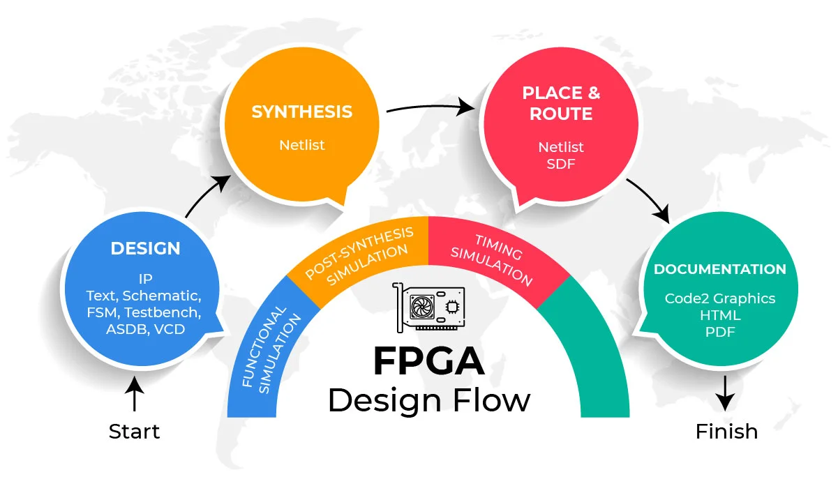
Design Specification → Define requirements.
Design Entry → Write HDL code or create schematics.
Simulation → Verify functionality.
Synthesis → Convert HDL to a netlist.
Place and Route → Map the design to FPGA resources.
Timing Analysis → Ensure timing constraints are met.
Bitstream Generation → Create the configuration file.
Burning → Load the configuration onto the FPGA.
Testing → Validate on hardware.
Optimization → Refine the design.
This process ensures a systematic approach to designing, verifying, and implementing FPGA-based systems.
