Time: 2025-03-06 11:49:43View:
Hot Swap technology is a critical feature in many electronic systems, particularly those requiring high reliability and minimal downtime, such as servers, networking equipment, and industrial systems. When applied to Xilinx FPGAs, Hot Swap technology enables the insertion and removal of FPGA-based boards or modules while the system is powered on, without causing disruptions or damage. Below is an analysis of how Hot Swap technology is applied in Xilinx FPGAs, its benefits, and implementation considerations.
Hot Swap refers to the ability to replace or add hardware components to a system without powering it down. This is achieved through careful design of the power delivery, signal integrity, and control logic to ensure safe insertion and removal of components.
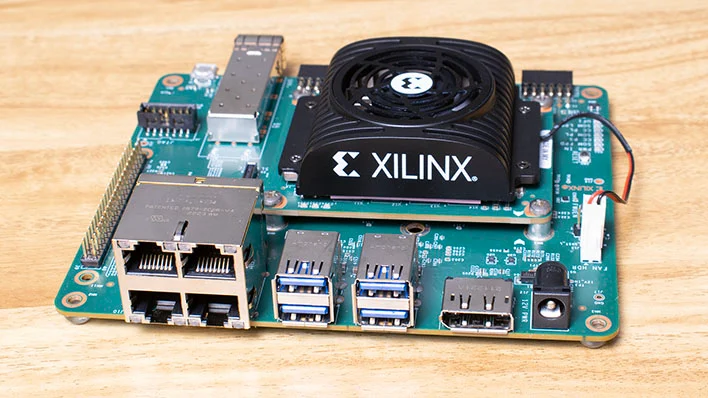
Xilinx FPGAs, such as those in the Virtex, Kintex, and Zynq families, are often used in systems where Hot Swap capability is essential. The technology is implemented through a combination of hardware and firmware techniques:
Hot Swap Controllers: External ICs or integrated logic to manage power sequencing and inrush current during board insertion.
Power Sequencing: Ensures that the FPGA's power rails are applied in the correct order during insertion.
I/O Protection: Prevents damage to FPGA pins during hot insertion by ensuring signals are not driven until power is stable.
Soft Start: Limits inrush current to avoid voltage droops or system instability.
Pre-Charge Circuits: Gradually charge capacitors on the board to avoid sudden current spikes.
1. System Availability:
Enables maintenance, upgrades, or replacements without shutting down the entire system.
Critical for high-availability systems like data centers or telecommunications.
2. Fault Tolerance:
Allows faulty FPGA-based boards to be replaced without affecting the rest of the system.
3. Scalability:
Facilitates the addition of new FPGA-based modules to expand system capabilities.
4. Protection:
Prevents damage to the FPGA, connectors, and other components during insertion or removal.
Implementing Hot Swap technology in Xilinx FPGAs requires careful design at both the hardware and firmware levels:
Power Management:
Use Hot Swap controllers (e.g., TI TPS2490, Analog Devices LTC4221) to manage power sequencing and inrush current.
Ensure proper power rail sequencing (e.g., VCCINT, VCCAUX, VCCO) as specified in the FPGA datasheet.
I/O Protection:
Use series resistors, diodes, or FETs to protect FPGA pins from voltage spikes during insertion.
Implement pre-charge circuits to gradually charge board capacitors.
Connector Design:
Use staggered connectors to ensure power and ground pins make contact before signal pins during insertion.
ESD Protection:
Add ESD protection devices to safeguard the FPGA and other components.
Power-On Reset (POR):
Ensure the FPGA's configuration logic is reset properly during power-up.
Use the FPGA's internal POR circuit or an external reset controller.
Configuration Management:
Use Xilinx's Partial Reconfiguration feature to dynamically update the FPGA's functionality without a full reset.
Implement robust error detection and recovery mechanisms.
Signal Integrity:
Ensure that signals are tri-stated or driven to safe levels during insertion.
Use Xilinx's I/O Buffer (IOB) features to control signal states.
Here’s an example of how Hot Swap can be implemented in a Xilinx FPGA-based system:
Hot Swap Controller: TI TPS2490 to manage 12V power rail.
Power Sequencing: Use a PMIC (e.g., Xilinx Power Estimator tool) to sequence VCCINT, VCCAUX, and VCCO.
Pre-Charge Circuit: Add a resistor and FET to limit inrush current during insertion.
Power-On Reset: Use the FPGA's internal POR circuit to initialize the device.
Configuration: Load the FPGA bitstream from an external flash memory or via JTAG.
I/O Control: Tri-state all I/O pins during insertion and enable them after power stabilization.
Inrush Current:
Challenge: Sudden current spikes during insertion can cause voltage droops.
Solution: Use soft-start circuits and Hot Swap controllers to limit inrush current.
Signal Integrity:
Challenge: Floating or improperly driven signals can cause damage.
Solution: Use series resistors and tri-state buffers to protect I/O pins.
Thermal Management:
Challenge: Hot-swapped boards may have different thermal profiles.
Solution: Monitor FPGA temperature using on-chip sensors and adjust cooling as needed.
Configuration Stability:
Challenge: Bitstream corruption during hot insertion.
Solution: Use error detection and correction (ECC) in the configuration memory.
Xilinx Vivado Design Suite: For FPGA configuration and partial reconfiguration.
Xilinx Power Estimator: To design power sequencing circuits.
Hot Swap Controllers: TI, Analog Devices, and Maxim Integrated offer dedicated ICs.
Xilinx Application Notes: Provide guidelines for Hot Swap implementation.
Hot Swap technology is a powerful feature for systems using Xilinx FPGAs, enabling high availability, fault tolerance, and scalability. By carefully designing the power delivery, I/O protection, and firmware logic, engineers can ensure safe and reliable operation during board insertion and removal. This capability is particularly valuable in mission-critical applications where system downtime is not an option.
