Time: 2025-03-21 11:12:31View:
The Xilinx 7 Series FPGAs (Field-Programmable Gate Arrays) are a family of programmable logic devices designed by Xilinx. The naming convention for these devices follows a specific pattern that provides information about the device's features, capabilities, and package. Here's a breakdown of the naming convention:
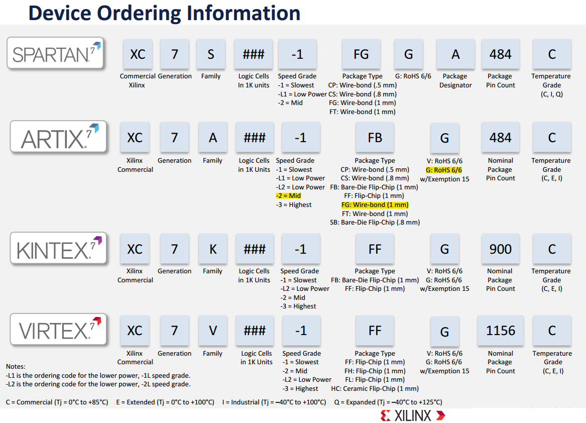
The naming convention for Xilinx 7 Series FPGAs typically follows this structure:
XC7<Family><Logic Cells><Package><Speed Grade><Temperature Grade><Optional Suffix>
1. XC7:
Indicates that the device belongs to the Xilinx 7 Series family.
2. <Family>:
A: Artix-7 (low-cost, low-power FPGAs).
K: Kintex-7 (mid-range FPGAs with a balance of performance and cost).
V: Virtex-7 (high-performance FPGAs for advanced applications).
Z: Zynq-7000 (SoC devices with an ARM processor and FPGA fabric).
Represents the specific sub-family within the 7 Series:
3. <Logic Cells>:
Represents the approximate number of logic cells in the device. This is a rough indicator of the device's capacity.
Examples: 35T, 100T, 200T, 485T, etc.
The number indicates the relative size of the FPGA fabric (e.g., 35T = 35,000 logic cells).
4. <Package>:
Indicates the type of package used for the device.
Examples: FGG484, FFG676, FBG676, etc.
The letters and numbers describe the package type, pin count, and ball grid array (BGA) configuration.
5. <Speed Grade>:
-1: Slowest speed grade.
-2: Medium speed grade.
-3: Fastest speed grade.
Represents the performance grade of the device:
Higher speed grades offer better performance but may consume more power.
6. <Temperature Grade>:
C: Commercial temperature range (0°C to 85°C).
I: Industrial temperature range (-40°C to 100°C).
Q: Extended temperature range (military/aerospace applications).
Indicates the operating temperature range of the device:
7. <Optional Suffix>:
ES: Engineering Sample (pre-production devices).
EV: Evaluation version.
L: Low-power variant.
Additional information, such as:
Let’s decode an example part number: XC7K325T-2FFG900C
XC7: Xilinx 7 Series FPGA.
K: Kintex-7 family.
325T: Approximately 325,000 logic cells.
2: Speed grade 2 (medium performance).
FFG900: Package type (FFG = Fine-pitch Ball Grid Array, 900 pins).
C: Commercial temperature range (0°C to 85°C).
The naming convention provides a quick way to identify the device's family, size, package, speed, and temperature range.
Understanding the naming convention helps in selecting the right FPGA for your application based on performance, power, and environmental requirements.
A minimum system for a Xilinx 7 Series FPGA typically includes the following components:
FPGA: Select a Xilinx 7 Series FPGA based on your application requirements (e.g., XC7A35T for low-cost applications).
Power Supply: Provide stable power to the FPGA. The 7 Series FPGAs require multiple voltage rails:
VCCINT: Core voltage (typically 1.0V for Artix-7/Kintex-7, 0.9V for Virtex-7).
VCCAUX: Auxiliary voltage (typically 1.8V or 2.5V).
VCCO: I/O bank voltage (depends on the I/O standard, e.g., 3.3V, 2.5V, 1.8V).
VCCBRAM: Block RAM voltage (typically 1.0V).
Clock Source: Provide a stable clock signal (e.g., 50 MHz oscillator).
Configuration Memory: Store the FPGA bitstream (e.g., SPI flash memory like Micron N25Q128).
JTAG Interface: For programming and debugging (using a JTAG cable like Xilinx Platform Cable USB II).
SPI Flash: For storing the FPGA configuration bitstream. The FPGA loads the bitstream from the flash at startup.
LEDs and Switches: For basic input/output testing.
Headers: For connecting external peripherals or expansion boards.
JTAG Header: Connect a JTAG programmer to configure and debug the FPGA.
UART Interface: For serial communication with a PC or other devices.
Use voltage regulators (e.g., LDOs or switching regulators) to generate the required voltage rails.
Ensure proper decoupling capacitors are placed near the FPGA pins to stabilize the power supply.
Connect a crystal oscillator or clock generator to the FPGA's global clock input pin (GCLK).
Connect the SPI flash memory to the FPGA's configuration pins (e.g., DIN, DOUT, CCLK, CS).
Add a JTAG header for programming and debugging.
Connect LEDs, switches, and headers to the FPGA's I/O pins.
Use pull-up or pull-down resistors as needed.
Design a PCB with proper routing for power, ground, and signal traces.
Follow Xilinx's guidelines for PCB layout (e.g., decoupling, signal integrity).
Use Xilinx Vivado or ISE to create and compile your FPGA design.
Program the FPGA via JTAG or SPI flash.
Test the system using basic logic (e.g., blink an LED).
Here’s an example of a minimum system for an XC7A35T-1FGG484C FPGA:
1. Power Supply:
VCCINT: 1.0V (using a switching regulator like TPS54620).
VCCAUX: 1.8V (using an LDO like LM1117-1.8).
VCCO: 3.3V (using an LDO like LM1117-3.3).
2. Clock Circuit:
50 MHz crystal oscillator connected to GCLK.
3. Configuration Memory:
SPI flash (e.g., Micron N25Q128) connected to FPGA configuration pins.
4. JTAG Interface:
6-pin JTAG header connected to FPGA's JTAG pins.
5. I/O Interfaces:
4 LEDs connected to FPGA I/O pins.
4 switches connected to FPGA I/O pins.
UART header for serial communication.
6. PCB Design:
4-layer PCB with proper power and ground planes.
Decoupling capacitors placed near each FPGA power pin.
Xilinx Vivado: For FPGA design, synthesis, and implementation.
Xilinx ISE: For older designs (deprecated for 7 Series but still usable).
JTAG Programmer: Xilinx Platform Cable USB II or compatible.
SPI Flash Programmer: To program the configuration memory.
By following these steps, you can build a functional minimum system for a Xilinx 7 Series FPGA. This system can serve as a foundation for more complex designs and applications.
