I. Introduction
Overview of Electronic Manufacturing Evolution
The evolution of electronic manufacturing has been marked by significant advancements in technology, leading to smaller, more efficient, and more powerful electronic devices. This transformation has been driven by the need for increased functionality, higher performance, and reduced costs in consumer, industrial, and military applications. Traditional through-hole technology (THT) has largely given way to more advanced techniques, such as Surface Mount Technology (SMT), which allows for the placement of components directly onto the surface of printed circuit boards (PCBs).
Importance of SMT and SMD in Modern Electronics
Surface Mount Technology (SMT) and Surface Mount Devices (SMD) are at the core of modern electronics manufacturing. SMT is the method used to place and solder SMDs onto PCBs. This technology is essential for producing compact, reliable, and high-performance electronic devices. SMT and SMDs offer several advantages over traditional through-hole components, including:
- Reduced Size and Weight: SMT allows for denser packing of components, leading to smaller and lighter devices.
- Higher Component Density: More components can be placed on a single PCB, enhancing functionality and performance.
- Improved Performance and Reliability: SMT components typically have better electrical performance and reliability due to shorter interconnections.
Automated Manufacturing: SMT lends itself well to automated processes, increasing production speed and consistency while reducing labor costs.
II. Definitions and Basic Concepts
Surface Mount Technology (SMT)
Definition
Surface Mount Technology (SMT) is a method for producing electronic circuits in which the components are mounted or placed directly onto the surface of printed circuit boards (PCBs). SMT components are soldered onto the board and do not require holes to be drilled through the PCB, unlike through-hole technology.
Historical Context
SMT began gaining prominence in the 1980s as a result of the growing demand for more compact, reliable, and cost-effective electronic devices. The shift from through-hole technology to SMT allowed manufacturers to produce smaller and more complex circuitry with higher component density, which in turn enabled the development of modern electronics such as smartphones, computers, and various other digital devices.
Basic Principles
- Component Placement: SMT involves placing components (SMDs) directly onto the PCB surface. This is typically done using automated machines that can precisely position the components.
- Soldering: Once positioned, the components are soldered to the board using reflow soldering or wave soldering techniques. Solder paste is applied to the PCB pads before component placement, and heat is used to melt the solder, forming a secure electrical connection.
- Inspection and Testing: After soldering, the assembled boards are inspected for defects and tested to ensure proper functionality.
Surface Mount Device (SMD)
Definition
A Surface Mount Device (SMD) is an electronic component that is designed to be placed and soldered directly onto the surface of a PCB. SMDs come in a variety of shapes and sizes, and they are characterized by having small leads or no leads at all, making them suitable for high-density mounting.
Comparison with Through-Hole Components
- Size and Weight: SMDs are generally smaller and lighter than through-hole components, which allows for more compact and lightweight designs.
- Assembly Process: SMDs are placed and soldered on the surface of the PCB, whereas through-hole components require holes to be drilled and their leads to be inserted through the PCB before soldering.
- Performance: SMDs often provide better electrical performance due to shorter interconnections and reduced parasitic inductance and capacitance.
- Reliability: SMDs typically offer higher reliability in high-vibration and high-frequency environments due to their robust attachment to the PCB surface.
Common Types
- Resistors: SMD resistors are available in various sizes and resistance values, typically marked with a standard code to indicate their resistance.
- Capacitors: SMD capacitors come in different types, such as ceramic, tantalum, and electrolytic, each with distinct characteristics and applications.
- Diodes: SMD diodes include signal diodes, Zener diodes, and light-emitting diodes (LEDs), used for rectifying, voltage regulation, and illumination.
- Transistors: SMD transistors, including bipolar junction transistors (BJTs) and field-effect transistors (FETs), are used for amplification and switching purposes.
Integrated Circuits (ICs): SMD ICs encompass a wide range of functions, from simple logic gates to complex microprocessors and memory chips.
III. Detailed Comparison: SMT vs. SMD
Conceptual Differences
What is SMT?
Surface Mount Technology (SMT) is a manufacturing process used in the production of electronic circuits. It involves the placement and soldering of components directly onto the surface of printed circuit boards (PCBs). SMT is a methodology that encompasses the entire manufacturing process, including component placement, soldering, and quality control.
Key aspects of SMT:
- It's a manufacturing technique, not a component type.
- It involves specialized equipment for component placement and soldering.
- SMT allows for higher component density and more compact designs.
- It's widely used in modern electronics manufacturing due to its efficiency and cost-effectiveness.
What is SMD?
Surface Mount Device (SMD) refers to the electronic components designed to be used with Surface Mount Technology. These components are specifically manufactured to be mounted directly onto the surface of PCBs without the need for through-holes.
Key aspects of SMDs:
- They are physical components, not a process.
- SMDs are designed with small form factors and flat contacts or short leads.
- They come in various types, including resistors, capacitors, diodes, and integrated circuits.
SMDs are optimized for automated placement and soldering in SMT processes.
Functional and Application Differences
Role in Manufacturing Process
SMT:
- Defines the overall manufacturing approach.
- Involves processes such as solder paste application, component placement, reflow soldering, and inspection.
- Requires specialized equipment like pick-and-place machines and reflow ovens.
- Focuses on efficiency, precision, and high-volume production.
SMD:
- Represents the components used within the SMT process.
- Designed for compatibility with automated placement and soldering techniques.
- Come in standardized packages for ease of handling and consistency in manufacturing.
Types of Devices and Components
SMT:
- Not applicable, as SMT is a process, not a type of device.
- However, SMT can be applied to various board types and designs, from simple single-layer PCBs to complex multi-layer boards.
SMD:
- Passive components: resistors, capacitors, inductors.
- Active components: diodes, transistors, LEDs.
- Integrated circuits: microcontrollers, memory chips, analog ICs, digital ICs.
- Electromechanical components: switches, connectors.
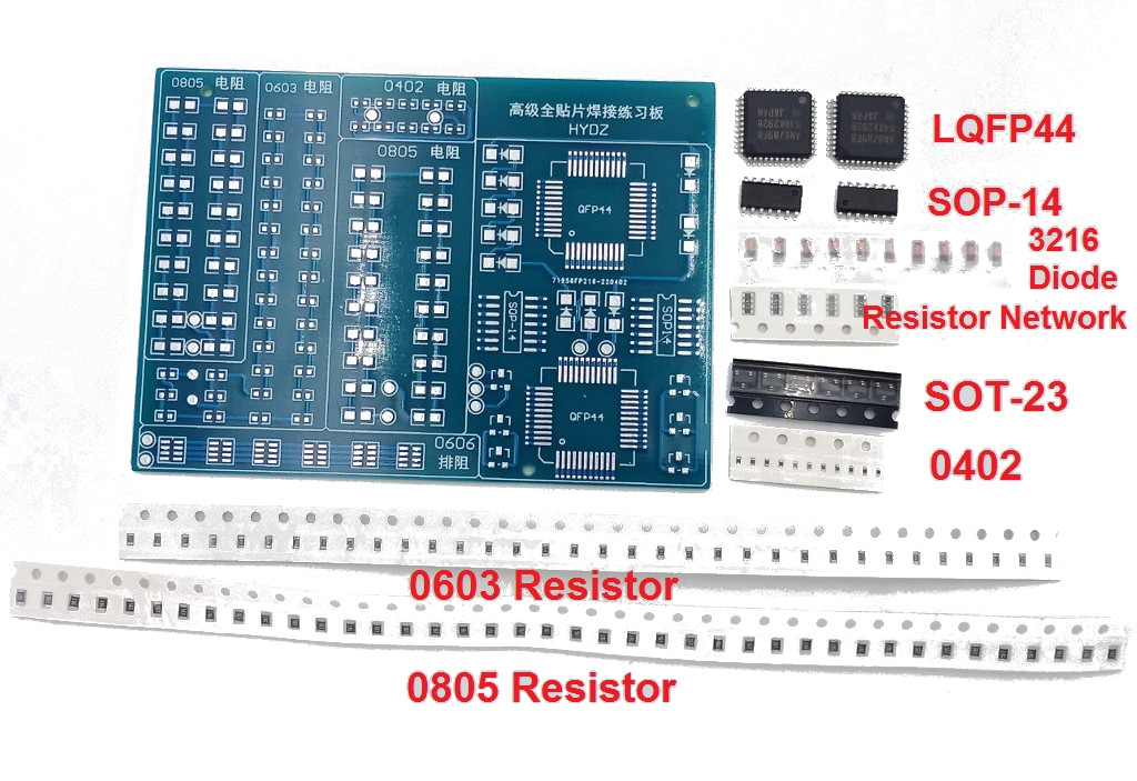
- Each type comes in various package styles (e.g., SOT, SOIC, BGA, QFP) optimized for different applications and density requirements.
Interrelation and Synergy in Electronics Manufacturing
SMT and SMD are inherently interconnected and synergistic in modern electronics manufacturing:
Complementary Relationship: SMT is the process that enables the efficient use of SMDs. Conversely, the development of SMDs has driven advancements in SMT processes.
Design Considerations: PCB designers must consider both SMT manufacturing capabilities and available SMD components when creating circuit layouts.
Miniaturization: The compact nature of SMDs allows for the full potential of SMT to be realized, enabling the production of smaller, more complex electronic devices.
Automation: SMDs are designed with features that facilitate automated handling and placement, which is a key aspect of SMT manufacturing.
Cost Efficiency: The combination of SMT processes and SMD components leads to more efficient use of board space, reduced material costs, and higher production speeds.
Technological Advancement: Improvements in SMD design (e.g., smaller packages, better thermal properties) often drive enhancements in SMT processes, and vice versa.
Quality and Reliability: The precision of SMT processes, combined with the robust design of SMDs, results in higher quality and more reliable electronic assemblies.
IV. In-Depth Analysis of SMT Technology
SMT Process Workflow
PCB Design and Fabrication
- PCB Design: The design phase involves creating a detailed layout of the circuit, specifying the positions of components, and defining the electrical connections. Design software (e.g., Altium, Eagle) is used to create a schematic and convert it into a PCB layout.
- Fabrication: The designed PCB is then manufactured, typically involving processes like photolithography, etching, plating, and drilling. The resulting board has copper traces and pads where components will be mounted.
Solder Paste Application
- Solder Paste Stenciling: A stencil with openings corresponding to the component pads on the PCB is placed over the board. Solder paste, a mixture of flux and tiny solder balls, is applied over the stencil and spread with a squeegee, filling the openings.
- Stencil Removal: The stencil is removed, leaving solder paste deposits on the PCB pads, ready for component placement.
Component Placement
- Pick-and-Place Machines: Automated machines pick components from reels or trays and precisely place them onto the PCB, aligning them with the solder paste deposits. These machines use vision systems to ensure accurate placement.
Reflow Soldering
- Reflow Oven: The PCB with placed components is passed through a reflow oven, which heats the board in a controlled manner. The solder paste melts and forms solder joints, securing the components to the PCB. The oven has multiple heating zones to ensure proper temperature profiles.
Inspection and Testing
- Automated Optical Inspection (AOI): AOI tools use cameras and image processing to inspect the solder joints and component placements for defects such as misalignment, insufficient solder, or solder bridges.
- Electrical Testing: Functional testing ensures that the assembled PCB operates as intended. This can include in-circuit testing (ICT) and functional testing (FT).
SMT Equipment and Tools
Solder Paste Printers
- Function: Solder paste printers apply solder paste to the PCB through a stencil. They ensure precise and consistent deposition of solder paste, which is crucial for reliable solder joints.
- Key Features: High accuracy, repeatability, and the ability to handle various stencil types and thicknesses.
Pick-and-Place Machines
- Function: These machines automatically place SMDs onto the PCB. They are capable of handling a wide range of component sizes and shapes with high speed and accuracy.
- Key Features: Vision systems for alignment, high-speed placement heads, and the ability to handle multiple component types simultaneously.
Reflow Ovens
- Function: Reflow ovens solder the components to the PCB by heating the board to melt the solder paste. They ensure a controlled thermal profile to avoid damaging components.
- Key Features: Multiple heating zones, precise temperature control, and conveyor systems for continuous processing.
Automated Optical Inspection (AOI) Tools
- Function: AOI tools inspect the assembled PCBs for defects. They use high-resolution cameras and image processing algorithms to detect issues such as solder bridges, missing components, and misalignments.
- Key Features: High inspection speed, accuracy, and the ability to adapt to different PCB designs.
Advantages and Challenges of SMT
Advantages
- High-Density Integration: SMT allows for the placement of more components on a smaller area, leading to compact and highly integrated designs.
- Automation and Efficiency: The SMT process is highly automated, resulting in faster production times, reduced labor costs, and consistent quality.
- Improved Performance: Shorter interconnections and lower parasitic inductance and capacitance improve the electrical performance of SMT assemblies.
- Cost-Effectiveness: Despite the high initial investment, SMT can reduce overall production costs through automation and efficient use of materials.
Challenges
- High Initial Investment: Setting up an SMT production line requires significant investment in equipment and technology.
- Maintenance Requirements: SMT equipment requires regular maintenance to ensure consistent performance and avoid downtime.
- Difficulty in Rework and Repair: SMT assemblies can be challenging to rework and repair due to the small size of components and the dense packing on the PCB.
SMT Applications in Various Industries
Consumer Electronics
- Applications: Smartphones, tablets, laptops, wearables, home appliances.
- Benefits: Compact designs, high functionality, and cost-effective mass production.
Automotive Electronics
- Applications: Engine control units (ECUs), infotainment systems, safety systems, sensors.
- Benefits: Reliability in harsh environments, high integration for complex systems, and improved performance.
Medical Devices
- Applications: Diagnostic equipment, patient monitoring systems, portable medical devices.
- Benefits: Miniaturization for portable devices, reliability, and precision.
Aerospace and Defense
- Applications: Avionics, communications systems, navigation systems, defense electronics.
- Benefits: High reliability, robust performance in extreme conditions, and advanced functionality for mission-critical applications.
In summary, SMT technology plays a crucial role in modern electronics manufacturing, enabling the production of highly integrated, reliable, and cost-effective electronic devices across various industries. While there are challenges associated with implementing and maintaining SMT processes, the advantages in terms of performance, efficiency, and scalability make it an essential technology in the electronics industry.
V. Comprehensive Examination of SMD Components
Types of SMDs
Passive Components
- Resistors: SMD resistors are available in various sizes and resistance values, and are typically used to limit current, divide voltages, and pull-up/down circuits.
- Capacitors: SMD capacitors, such as ceramic, tantalum, and electrolytic capacitors, store and release electrical energy, filter signals, and stabilize power supply voltages.
- Inductors: SMD inductors are used in signal filtering, energy storage in power supplies, and noise suppression in electronic circuits.
Active Components
- Integrated Circuits (ICs): SMD ICs include microcontrollers, memory chips, analog ICs, and digital ICs, providing various functionalities like processing, storage, and signal conditioning.
- Transistors: SMD transistors, including bipolar junction transistors (BJTs) and field-effect transistors (FETs), are used for switching and amplification purposes.
- Diodes: SMD diodes, such as signal diodes, Zener diodes, and light-emitting diodes (LEDs), are used for rectification, voltage regulation, and illumination.
Connectors and Switches
- SMD connectors and switches facilitate connections between different parts of a circuit and provide user interfaces. Examples include board-to-board connectors, micro USB connectors, and tactile switches.
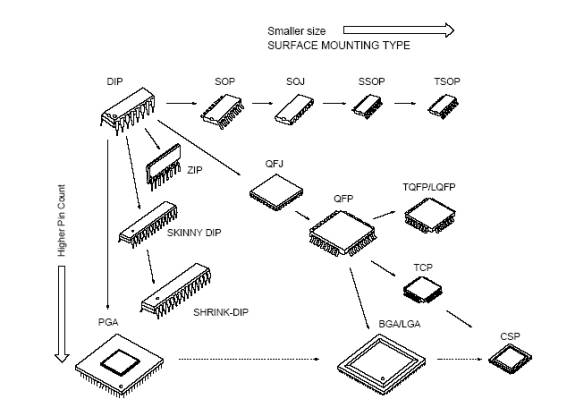
SMD Package Types
Chip Packages
- 0201, 0402, 0603, etc.: These numerical codes indicate the dimensions of passive components like resistors and capacitors in inches (e.g., 0603 means 0.06 inches by 0.03 inches).
Small Outline Packages
- SOIC (Small Outline Integrated Circuit): A type of IC package with gull-wing leads extending from the sides.
- SSOP (Shrink Small Outline Package): A smaller version of SOIC with tighter lead spacing.
- TSSOP (Thin Shrink Small Outline Package): Similar to SSOP but thinner.
Quad Flat Packages
- QFP (Quad Flat Package): An IC package with leads extending from all four sides.
- PLCC (Plastic Leaded Chip Carrier): A square or rectangular package with J-leads.
Advanced Packages
- BGA (Ball Grid Array): An IC package with solder balls on the underside, allowing for higher pin counts and better thermal performance.
- CSP (Chip Scale Package): A very small package, often just slightly larger than the die itself, used for high-density applications.
Emerging Packaging Technologies
- 3D Packaging: Stacking multiple ICs vertically to save space and improve performance.
- Fan-Out Wafer-Level Packaging (FOWLP): Extending the die area to allow more I/O connections without increasing the footprint.
- System in Package (SiP): Integrating multiple ICs and passive components into a single package to achieve a complete system.
Key Considerations for SMD Selection
Electrical Characteristics
- Voltage and Current Ratings: Ensure components can handle the required operating conditions.
- Tolerance and Stability: Precision and reliability under varying environmental conditions.
Thermal Performance
- Heat Dissipation: Components must be able to dissipate heat efficiently to avoid thermal damage.
- Thermal Resistance: Lower thermal resistance improves heat transfer.
Reliability
- Lifecycle and Durability: Consider the operational lifespan and failure rates.
- Environmental Tolerance: Resistance to factors like temperature, humidity, and mechanical stress.
Cost
- Component Cost: Balancing performance with budget constraints.
- Assembly Cost: Consider the impact on overall manufacturing costs, including equipment and labor.
Advantages and Challenges of SMDs
Advantages
- Miniaturization: SMDs enable the creation of smaller, more compact circuits.
- Lightweight: The reduced size and weight of SMDs contribute to lighter electronic devices.
- Superior Electrical Performance: Shorter interconnections reduce parasitic inductance and capacitance, improving performance.
- Thermal Management: Many SMD packages are designed for efficient heat dissipation.
Challenges
- Manual Soldering Difficulty: The small size of SMDs makes manual soldering challenging, requiring specialized tools and skills.
- Complexity in Rework and Replacement: High component density and small sizes complicate rework and repair processes.
- Initial Setup Costs: Implementing SMT and SMD technology requires significant investment in equipment and training.
- Inspection and Testing: Ensuring the quality of SMD assemblies can be more complex compared to through-hole technology.
VI. SMT and SMD in Manufacturing
PCB Design Considerations
Layout Optimization
- Component Placement: Arrange components to minimize signal path lengths and reduce crosstalk. Group related components together to streamline routing and reduce electromagnetic interference (EMI).
- Pad Design: Ensure proper pad size and spacing to accommodate SMDs, considering the specific package requirements of each component. This helps in achieving reliable solder joints.
- Routing: Optimize trace widths and spacing to handle current loads and signal integrity. Use multiple layers to separate power, ground, and signal traces effectively.
Impedance Control
- Controlled Impedance Traces: For high-frequency signals, design traces with controlled impedance to prevent signal reflections and ensure signal integrity.
- Differential Pairs: For differential signals, maintain consistent spacing and length matching between paired traces to preserve signal quality.
Thermal Management
- Heat Dissipation: Use thermal vias, copper pours, and heat sinks to manage heat dissipation. Place heat-generating components strategically to avoid hotspots.
- Thermal Relief: Design thermal reliefs for pads connected to large copper areas to facilitate soldering and prevent thermal stress.
Enhancing Production Efficiency
Automation and Flexible Manufacturing Systems
- Pick-and-Place Automation: Implement high-speed, high-precision pick-and-place machines to handle a variety of SMDs efficiently. Automation reduces human error and increases throughput.
- Flexible Manufacturing Systems (FMS): Use flexible manufacturing systems that can easily adapt to different PCB designs and production volumes. This enhances responsiveness to market demands and reduces downtime.
Production Line Optimization
- Line Balancing: Distribute tasks evenly across the production line to avoid bottlenecks. Optimize the placement of equipment to streamline the workflow.
- Lean Manufacturing: Apply lean manufacturing principles to eliminate waste, reduce setup times, and improve overall efficiency.
Quality Control Methods
- Automated Optical Inspection (AOI): Utilize AOI systems to inspect solder joints and component placements for defects. High-resolution cameras and image processing algorithms detect issues with high accuracy.
- X-Ray Inspection: Use X-ray inspection to evaluate solder joints, especially for hidden joints like those in BGA packages, to ensure reliability.
- In-Circuit Testing (ICT): Perform electrical testing on assembled PCBs to check for shorts, opens, and proper component values.
- Functional Testing (FT): Test the complete functionality of the assembled PCB to ensure it meets design specifications and operates as intended.
Cost Analysis
Material Costs
- Component Costs: SMD components can vary in cost depending on type, size, and specification. Bulk purchasing and supplier negotiation can help reduce costs.
- PCB Material: The choice of PCB material (e.g., FR4, high-frequency laminates) affects cost. High-quality materials may be more expensive but offer better performance and reliability.
Labor Costs
- Automation vs. Manual Labor: Investing in automation reduces labor costs in the long term, although there is an initial investment. Manual labor may be necessary for certain tasks, but it is more costly and less consistent.
- Training: Skilled labor is required for operating and maintaining SMT equipment. Training costs must be factored in to ensure proficiency and productivity.
Equipment Investment
- Initial Setup: The initial investment in SMT equipment, including pick-and-place machines, reflow ovens, and inspection systems, is significant but essential for high-volume, high-quality production.
- Depreciation: Consider the depreciation of equipment over time and plan for periodic upgrades to maintain production efficiency and capability.
Maintenance Costs
- Regular Maintenance: Routine maintenance of SMT equipment is critical to ensure reliable operation and minimize downtime. This includes servicing, calibration, and replacement of worn parts.
- Unexpected Repairs: Allocate budget for unexpected repairs and spare parts to avoid production delays.
VII. Future Trends and Innovations in SMT and SMD Technologies
Miniaturization and High-Density Integration
- Continued Miniaturization: The trend of making electronic devices smaller continues, pushing for further reduction in the size of SMD components and more densely packed PCBs.
- Ultra-Fine Pitch Technology: As device miniaturization progresses, the pitch of connections (distance between connection points on components and boards) becomes finer, requiring advancements in precision placement and soldering techniques.
3D Packaging Technologies
- Stacked Die Technologies: Multiple semiconductor dies stacked vertically within a single package, significantly increasing functionality without expanding footprint.
- Through-Silicon Vias (TSVs): Vias that go through the silicon wafer or die to provide connection between stacked chips, improving performance and reducing package size.
System-in-Package (SiP)
- Integration of Multiple Functions: SiP technology involves integrating multiple active electronic components into a single unit that performs all or most of the functions of an electronic system. SiP can include ICs, passive components, and even other SiPs.
Advanced Materials
- Conductive Polymers: Materials used to enhance the conductivity of electronic components while also offering flexibility, which is particularly useful in flexible and wearable electronics.
- Nanomaterials: Incorporating materials at the nanoscale to improve electrical, thermal, and mechanical properties of SMDs, such as carbon nanotubes and graphene.
Intelligent Manufacturing and Industry 4.0
- IoT in SMT Production: Integration of IoT devices in the SMT production line to monitor and optimize manufacturing processes in real time.
- AI and Machine Learning in Quality Control: Utilizing AI to enhance the precision and efficiency of quality control processes. Machine learning algorithms can predict and detect manufacturing anomalies early by analyzing data collected from sensors and cameras.
Environmental and Sustainability Considerations
- Lead-Free Soldering Techniques: Continued development of lead-free solder materials to meet environmental regulations and reduce health risks associated with lead.
- Use of Recyclable Materials: Increasing the use of recyclable or biodegradable materials in PCB manufacturing to minimize the environmental footprint of electronic waste.
Emerging Applications
- Flexible Electronics: Development of electronics that can bend, fold, or stretch, opening up applications in new areas such as flexible displays and electronic textiles.
- Wearable Devices: Advances in SMDs and integration technologies are enabling more sophisticated wearable devices, including health monitoring systems and smart clothing.
- 5G and Millimeter-Wave Technologies: As 5G networks roll out, there is an increasing demand for SMT and SMD technologies capable of handling high-frequency millimeter-wave components.
VIII. Case Studies
SMT/SMD Application in Consumer Electronics
Smartphones
- Miniaturization and Integration: The compact size of smartphones is made possible by SMT and SMD technologies, allowing manufacturers to fit a large number of components into a small form factor. Components such as microprocessors, memory chips, and sensors are all surface-mounted.
- High-Density PCBs: The use of multilayer PCBs and high-density interconnects (HDI) enables the integration of complex functionality, including communication modules, cameras, and power management circuits.
- Battery Management: SMD components play a crucial role in battery management systems, ensuring efficient power usage and charging.
Laptops
- Performance and Cooling: SMT allows for the placement of high-performance components like CPUs and GPUs. Efficient thermal management solutions, including heat sinks and thermal vias, are essential for maintaining performance.
- Connectivity: SMD connectors and ports (USB, HDMI, etc.) ensure robust and reliable connections for peripherals and external devices.
- Thin and Light Designs: The trend towards thinner and lighter laptops is facilitated by the compact nature of SMD components and the advanced packaging technologies used.
Wearables
- Compact and Lightweight: Wearable devices such as smartwatches benefit from the miniaturization of components, making them lightweight and comfortable to wear.
- Flexible Electronics: Some wearables use flexible PCBs and components to conform to different shapes, enhancing user comfort and functionality.
- Battery Efficiency: SMD components optimize power consumption, extending the battery life of wearables.
Automotive Electronics Solutions
Engine Control Units (ECUs)
- Robustness and Reliability: ECUs must withstand harsh automotive environments. SMT processes ensure reliable solder joints and component placement, critical for vehicle safety and performance.
- High-Temperature Components: Automotive-grade SMD components are designed to operate reliably at high temperatures and under mechanical stress.
Sensors
- Advanced Sensing: Automotive applications rely on a variety of sensors (e.g., temperature, pressure, proximity) that are surface-mounted for precise and reliable performance.
- Integration with Control Systems: SMD sensors are integrated into larger control systems to provide real-time data for vehicle operations such as braking, airbag deployment, and engine management.
Infotainment Systems
- High-Resolution Displays: The integration of high-resolution screens and user interfaces benefits from SMT technology, facilitating the use of thin and high-density PCBs.
- Connectivity: SMD components enable various connectivity options, including Bluetooth, Wi-Fi, and GPS, enhancing the infotainment experience.
Innovations in Medical Devices
Portable Medical Instruments
- Miniaturized Components: Portable medical devices, such as glucose meters and portable ECG monitors, use SMD components to achieve compactness and ease of use.
- Battery-Powered Efficiency: Efficient power management through SMD components ensures long battery life, which is crucial for portable medical devices used in remote or emergency situations.
Diagnostic Tools
- Precision and Accuracy: Diagnostic equipment, such as blood analyzers and imaging devices, rely on the precision and reliability of SMD components to deliver accurate results.
- Integration with IT Systems: SMD components facilitate the integration of diagnostic tools with healthcare IT systems, enabling real-time data sharing and analysis.
IX. Challenges and Solutions
Common Issues in SMT/SMD Processes
Solder Bridging
- Issue: Solder bridging occurs when solder paste connects adjacent pads, creating an unintended electrical connection.
- Solutions:
- Stencil Design: Optimize stencil aperture design to control the amount of solder paste deposited.
- Solder Paste Selection: Use solder paste with appropriate viscosity and particle size distribution.
- Reflow Profile: Fine-tune the reflow soldering profile to ensure proper melting and solidification of the solder.
Tombstoning
- Issue: Tombstoning is when one end of a component lifts off the PCB during reflow, resembling a tombstone.
- Solutions:
- Pad Design: Ensure balanced pad sizes and symmetrical solder paste deposits.
- Component Placement: Use proper placement pressure and alignment to keep components flat on the PCB.
- Reflow Profile: Optimize the thermal profile to achieve uniform heating and prevent uneven solder wetting.
Insufficient Solder
- Issue: Insufficient solder can lead to weak solder joints, resulting in poor electrical and mechanical connections.
- Solutions:
- Stencil Thickness and Aperture: Adjust the stencil thickness and aperture size to ensure adequate solder paste deposition.
- Solder Paste Application: Use automated solder paste printers for consistent and precise application.
- Inspection: Implement pre-reflow inspection to detect insufficient solder deposits early.
SMD-Specific Problems
Thermal Management
- Issue: High power density in SMDs can lead to overheating, affecting component reliability and performance.
- Solutions:
- Thermal Vias: Incorporate thermal vias to transfer heat from the component area to larger copper planes.
- Heat Sinks and Thermal Pads: Use heat sinks and thermal interface materials to dissipate heat efficiently.
- Component Placement: Place high-power components away from heat-sensitive areas and ensure adequate airflow.
Signal Integrity in High-Frequency Applications
- Issue: High-frequency signals are prone to issues like signal loss, crosstalk, and electromagnetic interference (EMI).
- Solutions:
- Controlled Impedance Traces: Design traces with controlled impedance to maintain signal integrity.
- Ground Planes and Shielding: Use continuous ground planes and EMI shielding to minimize interference.
- Differential Pair Routing: Maintain consistent spacing and length matching for differential pairs to reduce noise.
Strategies for Overcoming Challenges
Process Optimization
- Continuous Improvement: Implement a continuous improvement process to regularly review and enhance manufacturing procedures.
- Data Analytics: Use data analytics to identify and address process bottlenecks and defects.
- Standard Operating Procedures (SOPs): Develop and adhere to SOPs to ensure consistency and quality.
Training and Skill Development
- Employee Training: Regularly train employees on the latest SMT/SMD techniques, equipment operation, and troubleshooting methods.
- Certification Programs: Encourage certification through programs like IPC-A-610 for Acceptability of Electronic Assemblies.
- Cross-Training: Cross-train employees to handle various roles within the production line, enhancing flexibility and knowledge sharing.
Advanced Inspection Techniques
- Automated Optical Inspection (AOI): Use AOI systems for fast and accurate inspection of solder joints and component placement.
- X-Ray Inspection: Implement X-ray inspection, especially for hidden joints like BGA, to ensure solder joint integrity.
- In-Circuit Testing (ICT): Perform ICT to verify the electrical functionality of the assembled PCBs.
- Thermal Imaging: Use thermal imaging to detect hot spots and verify the effectiveness of thermal management solutions.
X. Conclusion
Summary of SMT and SMD Impact on Electronics Manufacturing
Surface Mount Technology (SMT) and Surface Mount Devices (SMD) have revolutionized electronics manufacturing, driving significant advancements in the miniaturization, functionality, and reliability of electronic products. These technologies have enabled manufacturers to produce highly integrated and complex devices, such as smartphones, laptops, automotive electronics, and medical instruments, with unprecedented efficiency and precision.
- Miniaturization: SMT and SMD have allowed for the reduction in size and weight of electronic devices, paving the way for compact and portable gadgets.
- High-Density Integration: The ability to place numerous components on a single PCB has enhanced the functionality and performance of electronic products.
- Automation: The automation of the SMT process has increased production speed, consistency, and reduced labor costs, making high-volume manufacturing more feasible.
- Improved Performance: Shorter interconnections and better thermal management facilitated by SMT and SMD components have led to superior electrical performance and reliability.
- Cost-Effectiveness: Despite the initial investment in equipment, the long-term benefits of reduced material costs, efficient use of space, and high production yields have made SMT a cost-effective choice for manufacturers.
Future Outlook and Opportunities
The future of SMT and SMD technologies is bright, with numerous opportunities for further innovation and growth:
- Continued Miniaturization: As the demand for smaller and more powerful devices grows, SMT and SMD technologies will evolve to support even greater levels of miniaturization and integration.
- 3D Packaging and Advanced Materials: Emerging packaging technologies, such as 3D packaging and the use of advanced materials like nanomaterials and conductive polymers, will further enhance the capabilities and applications of electronic devices.
- Intelligent Manufacturing: The adoption of Industry 4.0 principles, including the Internet of Things (IoT) and Artificial Intelligence (AI), will lead to smarter, more efficient manufacturing processes. Real-time monitoring, predictive maintenance, and AI-driven quality control will become standard practices.
- Environmental Sustainability: Increasing focus on environmental sustainability will drive the development of eco-friendly materials, lead-free soldering techniques, and recyclable components, reducing the environmental impact of electronics manufacturing.
- Emerging Applications: New and emerging applications, such as flexible electronics, wearable devices, and 5G/millimeter-wave technologies, will open up new markets and opportunities for SMT and SMD technologies.
