FPGA Design: The Complete Guide for Enthusiasts in 2024
Time: 2024-09-13 16:59:38View:
Introduction
Overview of FPGA Technology
Field-Programmable Gate Arrays (FPGAs) are semiconductor devices that can be programmed after manufacturing. They consist of an array of configurable logic blocks (CLBs) connected via programmable interconnects. FPGAs offer a unique combination of flexibility and performance, allowing designers to implement cust om digital circuits without the need for custom silicon fabrication.
Importance and Applications
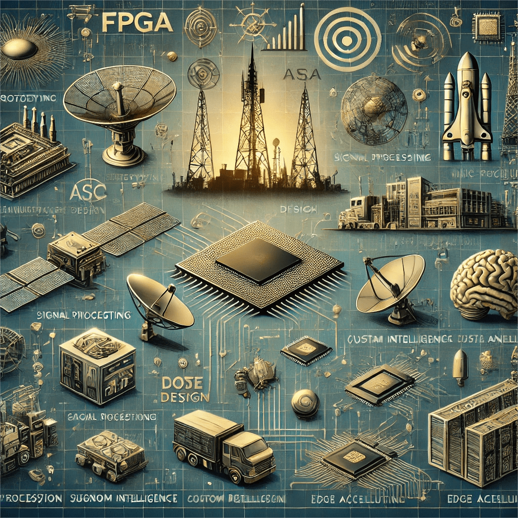
FPGAs have become increasingly important in various fields due to their versatility and ability to accelerate specific tasks. Some key applications include:
Prototyping: Rapid development and testing of ASIC designs
Signal Processing: Real-time processing for telecommunications and radar systems
Artificial Intelligence: Acceleration of machine learning algorithms
Data Centers: Custom accelerators for specific workloads
Aerospace and Defense: Reliable, radiation-tolerant computing solutions
Internet of Things (IoT): Edge computing and sensor fusion
Understanding FPGA Basics
Definition and Key Concepts
An FPGA is an integrated circuit designed to be configured by a customer or designer after manufacturing. Key concepts include:
Configurable Logic Blocks (CLBs): The basic building blocks of an FPGA, containing look-up tables (LUTs) and flip-flops
Programmable Interconnects: Routing resources that connect CLBs and other elements
I/O Blocks: Interfaces between the FPGA and external devices
Hard IP Cores: Pre-built, optimized circuits for common functions (e.g., memory controllers, high-speed transceivers)
Soft IP Cores: Pre-designed logic functions implemented using the FPGA's programmable fabric
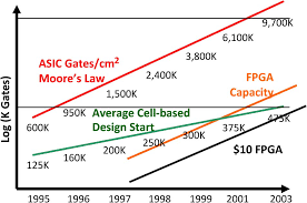
Historical Development
The evolution of FPGAs can be traced through several key milestones:
1984: Altera (now part of Intel) is founded
1985: Xilinx is founded and introduces the first commercial FPGA
1992: Introduction of SRAM-based FPGAs, improving reprogrammability
Late 1990s: Integration of hard IP cores begins
2000s: Adoption of high-level synthesis tools for easier design
2010s: Development of 3D IC technologies and system-on-chip (SoC) FPGAs
Present: Focus on AI acceleration and advanced packaging technologies
2. FPGA Architecture
FPGA architectures have evolved over time to meet various design requirements. The three main types of FPGA architectures are:
Symmetrical Array
Consists of a regular grid of logic blocks with horizontal and vertical routing channels
Offers high flexibility and is suitable for a wide range of applications
Examples: Many Xilinx and Intel (formerly Altera) FPGAs
Row-Based Architecture
Logic blocks are arranged in rows with horizontal routing channels between them
Vertical routing is achieved through dedicated interconnect lines
Can offer more efficient routing for certain types of designs
Examples: Some older Actel (now Microsemi) FPGAs
Hierarchical PLD
Combines elements of traditional PLDs with FPGA-like structures
Features a hierarchical arrangement of logic blocks
Can offer faster signal propagation for certain designs
Examples: Some Altera MAX series devices
Components of FPGA
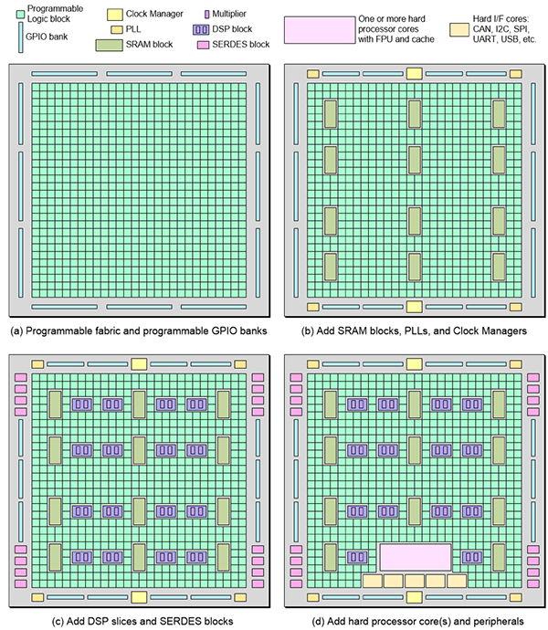
Modern FPGAs consist of several key components:
Configurable Logic Blocks (CLB)
The basic building blocks of an FPGA
Typically contain Look-Up Tables (LUTs), multiplexers, and flip-flops
Can be configured to implement various logic functions
Programmable Interconnects/Routing
Network of wires and programmable switches
Allows for flexible connections between CLBs and other components
Includes local, regional, and global routing resources
Input/Output Blocks (IOB)
Interface between the FPGA and external devices
Support various I/O standards and voltage levels
Often include features like serialization/deserialization (SerDes)
Block RAM (BRAM)
Dedicated memory blocks distributed throughout the FPGA
Can be used for data storage, FIFOs, and other memory-intensive functions
Offers higher performance and density compared to distributed RAM in CLBs
DSP Modules
Specialized blocks for digital signal processing operations
Typically include hardened multiply-accumulate (MAC) units
Enhance performance for applications like filtering and FFTs
Clock Management Resources
Include PLLs (Phase-Locked Loops) and DCMs (Digital Clock Managers)
Allow for clock generation, multiplication, division, and phase shifting
Crucial for managing clock domains and high-speed designs
Configuration Memory
Stores the FPGA's configuration data
Can be based on SRAM (volatile) or Flash (non-volatile) technology
Determines the behavior of CLBs, routing, and other components
3. FPGA vs. ASIC Design
Key Differences
Flexibility:
FPGA: Reprogrammable, allowing for post-production changes
ASIC: Fixed functionality after manufacturing
Performance:
FPGA: Generally lower performance due to programmable interconnects
ASIC: Higher performance, optimized for specific applications
Power Consumption:
FPGA: Higher power consumption due to programmable elements
ASIC: Lower power consumption, more energy-efficient
Cost:
FPGA: Lower upfront costs, higher per-unit costs for large volumes
ASIC: High initial costs (NRE), lower per-unit costs for large volumes
Time-to-Market:
FPGA: Faster development cycle, immediate prototyping
ASIC: Longer development cycle, requires fabrication
Three Reasons to Choose FPGA
Rapid Prototyping and Iteration:
FPGAs allow for quick design changes and updates, ideal for prototyping and evolving designs
Low-Volume or Uncertain Production Quantities:
FPGAs are cost-effective for low to medium production volumes, avoiding high ASIC NRE costs
Need for In-Field Updates:
FPGAs can be reprogrammed after deployment, allowing for bug fixes, feature updates, and adaptation to new standards
4. FPGA Development Process
The FPGA development process involves several key steps:
System Requirements Definition
Identify the overall system requirements and specifications
Define performance targets, power constraints, and interface requirements
Determine the system architecture and partitioning
Function Allocation to FPGA
Decide which functions will be implemented in the FPGA
Consider factors such as performance requirements, flexibility needs, and cost constraints
Determine if certain functions are better suited for software implementation (e.g., on a microprocessor)
Determining Required FPGA Features
Select the appropriate FPGA family based on the allocated functions
Consider factors such as:
Number of logic elements required
Memory requirements (Block RAM, distributed RAM)
I/O requirements and standards
Clock management needs
Specialized features (e.g., DSP blocks, high-speed transceivers)
Implementation
Develop the FPGA design using hardware description languages (HDL) or high-level synthesis tools
Follow the design workflow and methodologies (detailed in the next section)
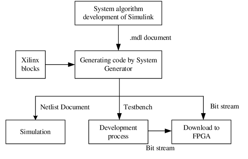
Design Workflow and Methodologies
Design Entry
Create the design using Hardware Description Languages (HDL) like VHDL or Verilog
Alternatively, use High-Level Synthesis (HLS) tools with languages like C/C++ or OpenCL
Develop or integrate IP cores for common functions
RTL Design and Simulation
Create Register Transfer Level (RTL) descriptions of the design
Perform functional simulation to verify design behavior
Use testbenches to provide input stimuli and check output responses
Synthesis
Convert RTL design into a netlist of FPGA primitives (e.g., LUTs, flip-flops)
Optimize the design for area, speed, or power consumption
Generate reports on resource utilization and timing estimates
Implementation (Place and Route)
Map the synthesized netlist to the specific FPGA architecture
Place the mapped elements onto the FPGA's physical resources
Route the connections between placed elements
Perform timing analysis and optimize to meet timing constraints
Testing and Debugging
Program the FPGA with the implemented design
Perform in-system testing and debugging
Use tools like Integrated Logic Analyzers (ILA) for real-time debugging
Iterate on the design if necessary
5. FPGA Program Memory
Types and Uses
Configuration Memory:
Stores the FPGA's configuration bitstream
Can be volatile (SRAM-based) or non-volatile (Flash-based)
Determines the functionality of the FPGA after power-up
User Memory:
Block RAM (BRAM): Dedicated memory blocks within the FPGA
Distributed RAM: Implemented using LUTs in the FPGA fabric
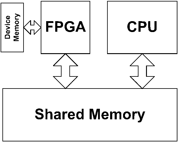
External Memory: Interfaced through I/O pins (e.g., DDR SDRAM)
Configuration Process
Power-Up:
FPGA enters configuration mode
Bitstream Loading:
Configuration data is loaded from an external source (e.g., flash memory, microcontroller) or through a programming interface (e.g., JTAG)
Initialization:
FPGA configures its internal components based on the loaded bitstream
Start-Up:
FPGA enters user mode, and the implemented design begins operation
6. FPGA Verification Process
Design and Synthesis Verification
Perform static timing analysis to ensure design meets timing constraints
Check for design rule violations
Verify synthesis results against RTL design
Simulation
Behavioral Simulation:
Verify functional correctness of the RTL design
Use testbenches to provide input stimuli and check outputs
Post-Synthesis Simulation:
Verify functionality after synthesis
Includes gate-level timing information
Post-Implementation Simulation:
Verify functionality after place and route
Includes detailed timing information and routing delays
Prototyping and Emulation
Use FPGA-based prototyping boards to verify the design in hardware
Employ hardware emulation systems for large or complex designs
Verify real-time performance and interaction with other system components
Lab Testing and Validation
Program the target FPGA with the final bitstream
Perform comprehensive functional testing in the target environment
Validate system-level performance and interactions
Conduct stress testing and corner case analysis
Verify compliance with relevant standards and specifications
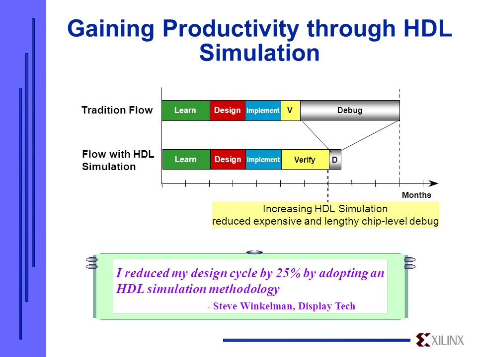
Advantages of FPGA Verification
FPGA verification offers several key advantages in the development process:
Early Error Detection
Identifies design flaws and bugs early in the development cycle
Reduces the cost and time associated with fixing issues later in the process
Allows for iterative refinement of the design before hardware implementation
Functional Verification
Ensures that the FPGA design behaves as intended under various conditions
Verifies correct operation of individual modules and their interactions
Helps in validating the design against system requirements and specifications
Timing Verification
Confirms that the design meets timing constraints and performance requirements
Identifies potential timing violations, such as setup and hold time issues
Helps in optimizing critical paths for better overall system performance
Formal Verification
Provides mathematical proof of design correctness
Verifies properties and assertions about the design
Helps in identifying corner cases and hard-to-find bugs that may be missed by simulation
7. FPGA Integration
Hardware Description Language (HDL) Design
HDLs are used to describe the structure and behavior of digital circuits
They allow for high-level abstraction of complex digital systems
HDLs support both behavioral and structural descriptions of hardware
VHDL and Verilog Overview
VHDL (VHSIC Hardware Description Language):
Strongly typed language with a syntax similar to Ada
Known for its verbosity and strong type checking
Popular in military and aerospace applications
Verilog:
C-like syntax, less verbose than VHDL
Weakly typed, offering more flexibility but potentially less safety
Widely used in industry, especially in ASIC design
Coding Best Practices
Modularity:
Design reusable, self-contained modules
Use clear, hierarchical structures
Synchronous Design:
Use synchronous logic wherever possible
Avoid combinational feedback loops
Clock Domain Crossing:
Use proper synchronization techniques when crossing clock domains
Parameterization:
Create flexible, scalable designs using parameters
Coding for Synthesis:
Follow coding styles that lead to efficient hardware implementation
Avoid constructs that may lead to inference of unnecessary hardware
Documentation and Commenting:
Provide clear, comprehensive comments in the code
Document design decisions, assumptions, and interfaces
Version Control:
Use version control systems to manage code revisions and collaborate effectively
8. Advantages and Disadvantages of FPGA
Advantages
Performance:
Ability to implement highly parallel architectures
Low latency due to hardware implementation
Can outperform general-purpose processors for specific tasks
Programmability:
Allows for in-field updates and modifications
Supports rapid prototyping and iterative development
Enables adaptation to changing requirements or standards
Cost-Effectiveness:
Lower non-recurring engineering (NRE) costs compared to ASICs
Economical for low to medium volume production
Reduces time-to-market for new products
Parallel Processing:
Can implement multiple independent processing units
Suitable for applications requiring high throughput
Enables efficient implementation of pipelined architectures
Disadvantages
Cost:
Higher unit cost compared to ASICs for high-volume production
Expensive for very large designs requiring high-end FPGAs
Power Consumption:
Generally higher power consumption compared to ASICs
Can be a limiting factor in battery-powered or energy-sensitive applications
Design Complexity:
Requires specialized knowledge of hardware design and FPGAs
Learning curve for software engineers transitioning to FPGA development
Debugging can be more challenging compared to software development
Performance Limitations:
Lower maximum clock speeds compared to ASICs
Potential for longer signal propagation delays due to programmable interconnects
Resource Constraints:
Fixed resources (LUTs, DSP blocks, memory) can limit design options
May require careful optimization to fit complex designs into available resources
9. FPGA vs. ASIC, PLD, Microcontrollers
Comparisons and Use Cases
FPGA vs. ASIC (Application-Specific Integrated Circuit):
FPGA: Prototyping, low to medium volume production, applications requiring field updates
ASIC: High-volume production, applications requiring maximum performance or minimum power consumption
Flexibility: FPGAs are reprogrammable, ASICs are fixed after manufacturing
Performance: ASICs generally offer higher performance and lower power consumption
Cost: FPGAs have lower upfront costs, ASICs are more cost-effective for high-volume production
Use cases:
FPGA vs. PLD (Programmable Logic Device):
FPGA: Complex digital systems, high-performance computing tasks
PLD: Simpler logic functions, glue logic, small-scale digital circuits
Complexity: FPGAs are more complex and versatile than traditional PLDs
Resources: FPGAs offer more logic resources and advanced features (e.g., DSP blocks, memory)
Use cases:
FPGA vs. Microcontrollers:
FPGA: High-speed data processing, custom digital interfaces, parallel computing tasks
Microcontroller: Embedded control systems, IoT devices, applications with simpler processing requirements
Architecture: FPGAs have a parallel architecture, microcontrollers are sequential
Flexibility: FPGAs offer hardware-level customization, microcontrollers are software-programmable
Ease of use: Microcontrollers are generally easier to program for software developers
Use cases:
10. FPGA Applications
FPGAs find applications in various industries due to their flexibility and performance. Here are some key application areas:
Aerospace and Defense
Radar signal processing
Software-defined radio
Satellite communications
Mission-critical systems with long lifecycles
Encryption and secure communications
Automotive
Advanced Driver Assistance Systems (ADAS)
In-vehicle infotainment systems
Engine control units
Vision systems for autonomous vehicles
High-speed data interfaces (e.g., GMSL, FPD-Link)
Data Centers
Network packet processing and routing
Data compression and encryption
Database acceleration
Machine learning inference acceleration
Custom accelerators for specific workloads
Medical Devices
Medical imaging systems (e.g., MRI, CT, Ultrasound)
Patient monitoring equipment
DNA sequencing and analysis
Real-time signal processing for diagnostic equipment
These applications leverage the key strengths of FPGAs, including:
Parallel processing capabilities
Ability to implement custom datapaths
Flexibility to adapt to evolving standards
High-speed interfaces for data-intensive applications
Low latency for real-time processing requirements
As technology advances, FPGAs continue to find new applications in emerging fields such as artificial intelligence, edge computing, and quantum computing simulation, further expanding their role in modern digital systems.
11. FPGA Design Examples and Best Practices
DSP with FPGA
Digital Signal Processing (DSP) is a key application area for FPGAs due to their parallel processing capabilities and dedicated DSP blocks.
Example: FIR Filter Implementation
vhdlCopylibrary IEEE;use IEEE.STD_LOGIC_1164.ALL;use IEEE.NUMERIC_STD.ALL;entity fir_filter is
    Port ( clk : in STD_LOGIC;
           x : in SIGNED(15 downto 0);
           y : out SIGNED(15 downto 0));end fir_filter;architecture Behavioral of fir_filter is
    type coefficient_array is array (0 to 3) of SIGNED(15 downto 0);
    constant coeffs : coefficient_array := (
        to_signed(16384, 16),  -- 0.5 in Q15 format
        to_signed(8192, 16),   -- 0.25 in Q15 format
        to_signed(4096, 16),   -- 0.125 in Q15 format
        to_signed(2048, 16)    -- 0.0625 in Q15 format
    );

    type delay_line is array (0 to 3) of SIGNED(15 downto 0);
    signal x_delayed : delay_line := (others => (others => '0'));
    begin
    process(clk)
        variable acc : SIGNED(31 downto 0);
    begin
        if rising_edge(clk) then
            -- Shift the delay line
            x_delayed <= x & x_delayed(0 to 2);

            -- Compute the filter output
            acc := (others => '0');
            for i in 0 to 3 loop
                acc := acc + x_delayed(i) * coeffs(i);
            end loop;

            -- Output the result (with rounding)
            y <= acc(30 downto 15) + acc(14);
        end if;
    end process;end Behavioral;
AI and Machine Learning
FPGAs are increasingly used for AI inference due to their ability to implement custom, parallel architectures.
Example: Simple Neuron Implementation
verilogCopymodule neuron #(
    parameter INPUT_SIZE = 4,
    parameter WEIGHT_WIDTH = 8,
    parameter ACTIVATION_WIDTH = 16)(
    input clk,
    input [INPUT_SIZE*WEIGHT_WIDTH-1:0] inputs,
    input [INPUT_SIZE*WEIGHT_WIDTH-1:0] weights,
    input [WEIGHT_WIDTH-1:0] bias,
    output [ACTIVATION_WIDTH-1:0] activation);

    reg [2*WEIGHT_WIDTH+$clog2(INPUT_SIZE)-1:0] sum;

    always @(posedge clk) begin
        sum <= 0;
        for (int i = 0; i < INPUT_SIZE; i = i + 1) begin
            sum <= sum + $signed(inputs[i*WEIGHT_WIDTH +: WEIGHT_WIDTH]) *
                         $signed(weights[i*WEIGHT_WIDTH +: WEIGHT_WIDTH]);
        end
        sum <= sum + (bias << $clog2(INPUT_SIZE));
    end

    // Simple ReLU activation function
    assign activation = (sum[2*WEIGHT_WIDTH+$clog2(INPUT_SIZE)-1]) ? 0 : sum[ACTIVATION_WIDTH-1:0];endmodule
Network and Communication Applications
FPGAs excel in networking applications due to their ability to process packets at line rate.
Example: Simple Packet Counter
verilogCopymodule packet_counter(
    input clk,
    input reset,
    input packet_valid,
    output reg [31:0] packet_count);

    always @(posedge clk or posedge reset) begin
        if (reset) begin
            packet_count <= 32'b0;
        end else if (packet_valid) begin
            packet_count <= packet_count + 1;
        end
    endendmodule
Best Practices for Code Readability and Performance Optimization
Use meaningful names for signals, variables, and modules
Comment your code thoroughly, explaining the purpose of each module and complex logic
Use parameterization to create flexible, reusable modules
Optimize for parallel processing by breaking down tasks into independent operations
Use pipelining to improve throughput in data-intensive applications
Leverage FPGA-specific features like DSP blocks and block RAMs when appropriate
Use timing constraints to guide the synthesis and implementation tools
Perform thorough simulation and timing analysis to ensure design correctness and performance
FAQ Section
Q: What's the difference between an FPGA and a CPU?
A: An FPGA is a reconfigurable hardware device that can implement custom digital circuits, while a CPU is a fixed-architecture processor that executes software instructions sequentially.
Q: Can FPGAs be programmed in high-level languages like C++?
A: While FPGAs are typically programmed using HDLs like VHDL or Verilog, there are High-Level Synthesis (HLS) tools that allow programming in C++ or other high-level languages, which are then converted to HDL.
Q: How do I choose between an FPGA and an ASIC for my project?
A: Consider factors like production volume, required performance, power constraints, and development time. FPGAs are better for low to medium volume, faster time-to-market, and designs that may need updates. ASICs are better for high volume production and when maximum performance or minimum power consumption is critical.
Q: What are the main challenges in FPGA design?
A: Common challenges include managing timing constraints, optimizing resource usage, dealing with tool complexities, and debugging hardware designs.
Q: How can I get started with FPGA development?
A: Start by learning a Hardware Description Language (HDL) like VHDL or Verilog. Then, acquire a development board and use vendor-provided tools to create and implement simple designs. Many FPGA vendors offer free or low-cost starter kits and online tutorials.
Conclusion
Recap of Key Points
FPGAs offer a unique combination of flexibility and performance, making them suitable for a wide range of applications.
The FPGA development process involves system requirements definition, function allocation, HDL coding, synthesis, implementation, and verification.
FPGAs excel in applications requiring parallel processing, custom data paths, and adaptability to changing standards.
Compared to ASICs, FPGAs offer lower non-recurring engineering costs and faster time-to-market, but may have higher unit costs and power consumption.
Best practices in FPGA design include modular design, efficient use of FPGA resources, and thorough verification at all stages of development.
Future Trends in FPGA Technology
Integration of AI and Machine Learning Accelerators: FPGAs are increasingly incorporating specialized AI engines to accelerate machine learning inference.
Heterogeneous Computing: Future FPGAs may integrate more diverse computing elements, such as GPUs or specialized processors, on the same chip.
Advanced Packaging Technologies: 3D stacking and chiplet technologies are enabling higher-density, higher-performance FPGA designs.
Higher-Level Design Abstractions: Tools for high-level synthesis and system-level design are evolving to make FPGA development more accessible to software engineers.
Edge Computing: FPGAs are finding new applications in edge devices, enabling low-latency processing for IoT and AI applications.
Quantum Computing Simulation: FPGAs may play a role in simulating and developing quantum computing algorithms.
Open-Source FPGA Ecosystems: There's a growing interest in open-source FPGA tools and even open-source FPGA hardware designs.
If you want to buy FPGA to start your business, vemeko can provide you with high quality FPGA chips