Time: 2024-10-08 17:34:12View:
FPGA (Field Programmable Gate Arra) is a flexible and powerful hardware device widely used in communication, embedded systems, and artificial intelligence. In this article, we will dive deep into the core concepts and common terminologies of FPGA, helping readers systematically understand various aspects of FPGA design.
FPGA is composed of multiple Configurable Logic Blocks (CLB), each containing Lookup Tables (LUT), flip-flops, and multiplexers. These CLBs can be configured into various logic circuits and connected through an interconnection mesh to realize complex logic functions. Other important resources include:
LUT (Look-Up Table): The basic unit used to implement logic functions. It stores logic combinations, similar to a truth table.
DSP Slice: Used for high-speed operations such as multiplication and addition, crucial for digital signal processing.
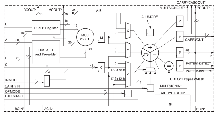
BRAM (Block RAM): On-chip memory used for buffering and storing data, featuring high efficiency and low latency.
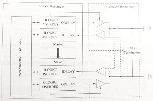
FPGA's input and output are managed through Input/Output Blocks (IOB) which communicate with external devices, supporting multiple interface standards such as LVDS, TTL, and LVCMOS. Additionally, the Phase-Locked Loop (PLL) can generate different frequency clock signals to ensure timing consistency among various modules.
IOB (Input/Output Block): The bridge for communicating with external circuits.
PLL (Phase-Locked Loop): Generates and adjusts clock signals of different frequencies, ensuring system synchronization.
FPGA development requires specialized software and languages to describe hardware structures and logic behavior. Common tools and technologies include:
HDL (Hardware Description Language): The core tool for FPGA programming, used to describe logic behavior. Verilog and VHDL are two commonly used HDLs.
Verilog: Known for its simplicity and C-like syntax, making it popular among beginners.
VHDL: Offers strong typing and a more formal syntax, preferred for critical applications.
Vivado/ISE/Quartus: Development software provided by Xilinx and Intel for designing, simulating, and synthesizing FPGA designs.
HLS (High-Level Synthesis): Generates HDL code from high-level languages (such as C/C++), accelerating development.
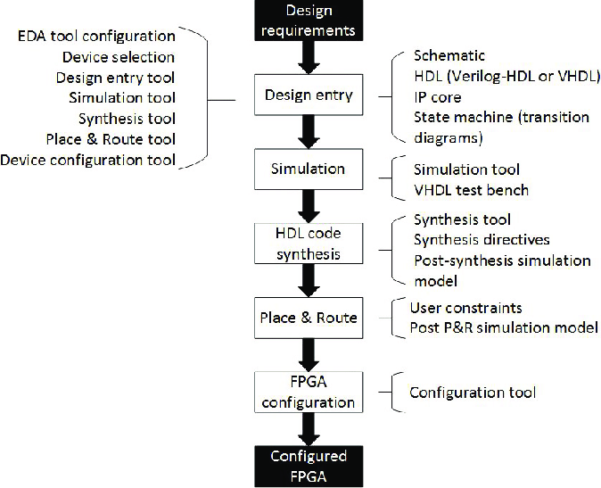
The FPGA design process involves multiple steps such as synthesis, placement and routing, and configuration. During the design process, handling timing, resource utilization, and integration of functional modules are crucial:
Place and Route: Maps the design onto the FPGA, arranging logic blocks and interconnections.
Timing Constraint: Ensures that circuits complete operations within specific timeframes, ensuring design stability.
Bitstream: The final generated configuration file containing the logic and connection information for FPGA.
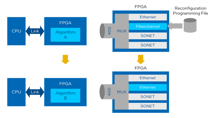
FPGA supports Partial Reconfiguration, which allows reconfiguring part of the chip while keeping other functions running. Additionally, a Soft Core Processor can be used to implement custom CPUs in FPGA, such as Xilinx's MicroBlaze.
-Partial Reconfiguration: Dynamically modifies part of the circuit for flexibility and resource optimization. A typical use case is changing the logic for different tasks without stopping the entire FPGA.
Soft Core Processor: A processor implemented in FPGA, allowing flexible customization of the processor core.
In FPGA, FIFO is commonly used between different modules for sequential data storage and cross-clock domain transfers. Proper handling of cross-clock domain data transfers is crucial to ensure data integrity:
FIFO (First In, First Out): Ensures sequential data transfer and consistency across clock domains.
Clock Domain Crossing (CDC): Handles data transfer between different clock domains, preventing system failures. Cross-clock domain transfers are prone to metastability, which can be mitigated by using FIFOs and synchronization techniques.
Resource utilization is an important metric to measure FPGA design, determining the design's size and performance. Designers need to optimize the design through timing constraints, multi-cycle paths, etc.:
Resource Utilization: Measures the use of logic resources (such as LUT, DSP, and BRAM) in FPGA.
Multicycle Path: Some calculations require multiple clock cycles to complete to meet timing requirements. Designers must ensure that these paths are properly constrained to avoid timing violations.
In FPGA development, developers often use pre-designed Intellectual Property (IP) cores that have been verified, allowing quick implementation of complex functions, such as Ethernet controllers and PCIe interfaces.
IP Core: Ready-made functional modules for accelerating development and functional integration. For example, a PCIe IP core allows fast data transfer between the FPGA and a computer without designing it from scratch.
Debugging and verification are indispensable steps in FPGA design. JTAG is a commonly used debugging interface that supports real-time monitoring and debugging of the internal logic of FPGA.
JTAG: Debugging and testing interface for online debugging and programming.
FPGA is widely used in communication, image processing, automotive electronics, and industrial control. Its high flexibility and parallel computing capability give it a unique advantage in scenarios requiring high-speed data processing and real-time response.
FPGA is particularly advantageous in applications like automotive electronics, where real-time data processing and rapid response are crucial, as well as in communication systems that require high-speed data transmission.
FPGA design requires developers to master hardware description languages, understand basic hardware architecture, and be proficient with various development tools and debugging techniques. Through this article, you have learned about the basic building blocks, design process, development tools, and application scenarios of FPGA, laying a solid foundation for further exploration of the FPGA world.
