Time: 2024-01-31 18:04:35View:
Timing closure is a critical step in the design and implementation of Field-Programmable Gate Arrays (FPGAs). In FPGA design, timing closure refers to the process of ensuring that the design meets all the required timing constraints. These constraints specify the maximum allowed delay from the input of a circuit to its output, and they are crucial for the correct operation of the design.
When designing an FPGA, engineers typically start with a high-level description of the desired functionality, often written in a hardware description language (HDL) such as VHDL or Verilog. This high-level description is then synthesized and mapped onto the target FPGA device, resulting in a netlist—a representation of the design in terms of logic gates and interconnections.
During the implementation phase, the netlist is further transformed into a configuration bitstream that can be loaded onto the FPGA to program its internal resources. However, this process introduces delays due to the inherent properties of the FPGA's programmable fabric and interconnect resources. These delays can cause timing violations, where the required timing constraints are not met.
Timing closure involves iteratively refining the design and making adjustments to eliminate timing violations. This process can be challenging because it requires a deep understanding of the FPGA architecture, the design's performance requirements, and the tools used for synthesis and place-and-route.
To achieve timing closure, designers employ various techniques. They can optimize the design by reducing the logic depth, minimizing fan-out and fan-in, and balancing the delays across critical paths. Additionally, they can use pipelining to break down long paths into smaller segments, which helps meet timing requirements. Another technique is to perform retiming, which involves moving registers within the design to better balance the delays.
Timing closure also involves careful consideration of the physical aspects of the design. Placement and routing play a crucial role in determining the delays in the interconnects. Designers may need to manually guide the placement of critical components to minimize delays and ensure timing closure. They can also use constraints and directives to guide the routing process.
The process of timing closure typically involves an iterative cycle of analysis and optimization. Designers analyze the timing reports generated by the synthesis and place-and-route tools and identify areas where timing violations occur. They then make adjustments to the design, such as modifying the logic or constraints, and rerun the implementation tools to verify if the changes have resolved the timing issues. This iterative process continues until all timing constraints are met, or a satisfactory compromise is reached.
In summary, timing closure is a crucial step in FPGA design to ensure that the design meets the required timing constraints. It involves a combination of architectural, logical, and physical optimizations to eliminate timing violations. Achieving timing closure requires a deep understanding of the FPGA architecture, the design's performance requirements, and the tools used for synthesis and place-and-route. Through careful analysis, optimization, and iteration, designers can successfully close timing and achieve reliable operation of their FPGA designs.
If we let the combinational logic delay = CLD, clock period = CLK, setup time = ST, hold time = HT, clock-to-Q propagation delay = CQ, then the following formula shows our constraints.
HT - CQ < CLD < CLK - CQ - ST

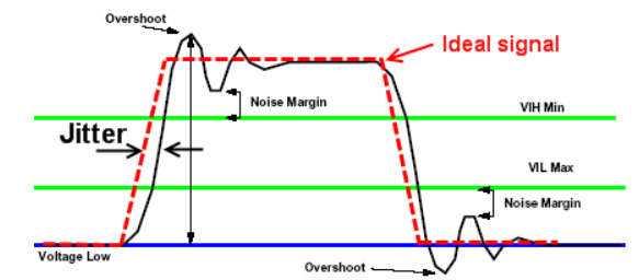
Clock jitter in FPGA refers to the variation or deviation in the timing of the clock signal within the FPGA fabric. FPGAs are programmable devices that consist of configurable logic blocks (CLBs), interconnect resources, and routing resources. The clock signal is distributed throughout the FPGA to synchronize the operation of various components and circuits.
Clock jitter in FPGAs can occur due to several factors, including noise sources, power supply fluctuations, electromagnetic interference, and imperfections in the clock generation circuitry. These factors can introduce timing uncertainties and distortions in the clock signal, leading to clock jitter.
Clock jitter in FPGAs can have a significant impact on the performance and reliability of the design. It can affect the setup and hold times of flip-flops and other sequential elements, potentially leading to timing violations and data errors. Jitter can also reduce the noise margins and degrade the signal integrity, making the design more susceptible to noise-induced errors.
To mitigate the effects of clock jitter in FPGAs, designers employ various techniques during the design and implementation process. One approach is to use low-jitter clock sources and clock conditioning circuits. These circuits can filter out noise and provide a cleaner and more stable clock signal to the FPGA fabric, reducing the impact of jitter.
Clock jitter in FPGAs can also be mitigated by careful clock routing and buffering. Designers can use dedicated clock routing resources and clock distribution networks within the FPGA fabric to minimize the introduction of jitter. By optimizing the placement of clock buffers and controlling the signal propagation delays, the skew and jitter can be reduced.
Furthermore, advanced clocking techniques such as phase-locked loops (PLLs) can be employed in FPGAs to reduce clock jitter. PLLs are feedback control systems that generate a stable clock signal by locking onto an input reference signal and dynamically adjusting its frequency and phase. PLLs can help to compensate for timing variations and reduce the effects of jitter in the clock signal.
During the design and implementation process, FPGA-specific tools and features can assist in analyzing and optimizing clock jitter. These tools can provide reports and analysis on the jitter characteristics of the clock signals, allowing designers to identify areas of excessive jitter and make appropriate adjustments. FPGA design tools may also offer options to optimize clock routing, apply clock skew adjustment techniques, and perform static timing analysis to ensure that the design meets timing requirements and minimizes the impact of jitter.
Accurate measurement and analysis of clock jitter in FPGAs are crucial for understanding its impact on system performance. Specialized test equipment, such as oscilloscopes and jitter analyzers, can be used to quantify and analyze the jitter characteristics of the clock signals. By characterizing the jitter, designers can make informed design decisions, apply appropriate optimizations, and ensure reliable operation of the FPGA design.
In summary, clock jitter in FPGAs refers to the variation or deviation in the timing of the clock signal within the FPGA fabric. It can be caused by noise, power supply fluctuations, electromagnetic interference, and imperfections in the clock generation circuitry. Clock jitter can impact the setup and hold times of sequential elements, reduce noise margins, and degrade signal integrity. To mitigate clock jitter, designers employ techniques such as low-jitter clock sources, clock conditioning circuits, careful clock routing, buffering, and advanced clocking techniques like PLLs. Accurate measurement and analysis of clock jitter are crucial for understanding its impact and making informed design decisions to ensure reliable operation of the FPGA design.

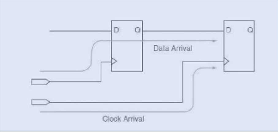
Clock skew in FPGA refers to the variation in arrival times of the clock signal at different elements or regions within the FPGA fabric. FPGAs consist of configurable logic blocks (CLBs), interconnect resources, and routing resources that are used to implement digital designs. The clock signal is distributed through these resources to synchronize the operation of the components within the FPGA.
Clock skew in FPGAs can occur due to various factors, including differences in routing delays, variations in interconnect lengths, and process variations during fabrication. These factors can lead to variations in the arrival times of the clock signal, causing clock skew.
Clock skew in FPGAs can have significant implications for the design's performance and functionality. It can affect the setup and hold times of flip-flops and other sequential elements, potentially leading to timing violations and data errors. Excessive clock skew can also result in violations of the maximum clock period, causing functional failures or incorrect operation of the design.
To mitigate clock skew in FPGAs, designers employ various techniques during the design and implementation process. One approach is to use dedicated clock distribution networks within the FPGA fabric. These networks consist of specialized routing resources, such as global clock lines and clock distribution trees, which are designed to minimize clock skew. By carefully routing the clock signals through these dedicated resources, the skew can be reduced.
Another technique is to use clock region constraints during the placement and routing phase of the design implementation. By specifying clock region constraints, designers can guide the placement of critical components and ensure that they are located in close proximity to each other, minimizing the effects of clock skew. Clock region constraints can also help in achieving better control over the routing of clock signals, further reducing skew.
In addition to using dedicated clock distribution networks and constraints, designers can utilize advanced FPGA-specific features to mitigate clock skew. These features may include global clock buffers, clock multiplexers, and clock skew adjustment circuits. Global clock buffers provide a low-skew distribution of the clock signal throughout the FPGA fabric. Clock multiplexers enable the selection of different clock sources for different regions of the design, allowing for better control of skew. Clock skew adjustment circuits can dynamically adjust the phase or delay of the clock signal to compensate for any residual skew.
During the implementation process, FPGA design tools also provide options to analyze and optimize clock skew. These tools generate reports that identify regions of the design where clock skew is high, allowing designers to make adjustments and optimizations to reduce skew. They may suggest modifications to the placement of critical components or provide guidance on routing strategies.
Accurate measurement and analysis of clock skew in FPGAs are crucial for understanding its impact on system performance. FPGA-specific tools and hardware debugging features, such as on-chip logic analyzers, can be used to measure and analyze the skew. By identifying areas of excessive skew, designers can make informed design decisions, apply appropriate optimizations, and ensure reliable operation of the FPGA design.
If we let clock skew = CS then the following formulas are updated versions of the previous ones.
CD > HT - CQ +/- CS
CLPD < CLK - CQ - ST +/- CS
In summary, clock skew in FPGAs refers to the variation in arrival times of the clock signal at different elements or regions within the FPGA fabric. It can result from routing delays, interconnect variations, and process variations. Clock skew can have significant implications for design performance and functionality. To mitigate clock skew, designers employ techniques such as dedicated clock distribution networks, clock region constraints, and FPGA-specific features. Accurate measurement and analysis of clock skew are crucial for identifying areas of excessive skew and making informed design decisions to ensure reliable operation of the FPGA design.

Achieving time closure in FPGA design is the process of ensuring that the design meets all timing requirements and constraints, thereby guaranteeing reliable and correct operation. It involves optimizing the design to meet setup and hold time requirements, minimizing clock skew and jitter, and resolving any timing violations. Here are several steps that can be taken to achieve time closure in FPGA design:
1. Define and analyze timing constraints: Start by defining accurate and realistic timing constraints for the design. Timing constraints specify the desired setup and hold times for the flip-flops and other sequential elements in the design. Analyze the timing constraints to ensure they are achievable and properly reflect the design requirements and performance goals.
2. Perform static timing analysis (STA): Use FPGA design tools to perform static timing analysis. STA analyzes the design's timing paths, taking into account the propagation delays of signals and the constraints specified. The analysis identifies timing violations, such as setup violations or hold violations, which indicate areas where the design is not meeting timing requirements. Analyze the timing reports to identify critical paths and understand the sources of timing violations.
3. Optimize placement and routing: The placement and routing of the design plays a crucial role in meeting timing requirements. Consider using placement constraints to guide the placement of critical components closer to each other, reducing signal propagation delays. Explore various routing strategies to minimize wire lengths and reduce signal delays. Utilize FPGA-specific features, such as dedicated clock routing resources and clock region constraints, to minimize clock skew and improve clock distribution.
4. Clock tree synthesis (CTS): Utilize clock tree synthesis algorithms provided by FPGA design tools to optimize the clock distribution network. CTS algorithms automatically generate a clock tree that balances the clock skew and ensures proper synchronization. This optimization helps to minimize clock skew and improve overall timing performance.
5. Timing-driven optimization: Apply timing-driven optimization techniques to improve the design's timing performance. These techniques involve automatically restructuring the design to reduce critical path delays. They may include logic restructuring, retiming, pipelining, or insertion of additional registers. Timing-driven optimization can help in resolving timing violations and meeting timing requirements.
6. Incremental design changes: Make incremental changes to the design and re-run the timing analysis after each change to evaluate the impact on timing closure. This iterative process allows you to identify the most effective optimizations and track the progress towards achieving time closure.
7. Clock skew and jitter management: Minimize clock skew and jitter by using low-jitter clock sources, clock conditioning circuits, careful clock routing, buffering, and advanced clocking techniques such as phase-locked loops (PLLs). Accurate measurement and analysis of clock skew and jitter using specialized tools can help identify areas of excessive skew or jitter and guide optimization efforts.
8. Iterative verification and validation: Conduct thorough functional verification and validation of the design to ensure that timing optimizations do not introduce functional errors. Use simulation, formal verification, and hardware testing to validate the design's functionality and performance.
9. Post-implementation timing analysis: After the design is implemented on the FPGA, perform post-implementation timing analysis to confirm that all timing requirements are met. This analysis provides a final verification of time closure and ensures that any implementation-specific factors are taken into account.
By following these steps and employing appropriate design techniques, such as careful constraint management, placement and routing optimization, timing-driven optimization, and clock skew/jitter management, FPGA designers can achieve time closure and ensure the design meets all timing requirements for reliable operation.