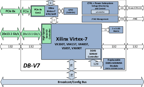
Xilinx's 7 Series FPGAs (Field-Programmable Gate Arrays) are part of the company's Artix-7, Kintex-7, and Virtex-7 families, which offer a wide range of performance, power efficiency, and cost-effective solutions for various applications. The architecture of the 7 Series FPGAs is designed to provide high flexibility, high performance, and lower power consumption compared to previous generations, making them suitable for applications such as communications, consumer electronics, industrial control, automotive, and military systems.

Below is an overview of the key architectural features of the Xilinx 7 Series FPGAs:
1. FPGA Architecture Overview
The 7 Series FPGAs use the UltraScale+ architecture, which includes several key components like:
- Logic Cells (LUTs, Flip-Flops, etc.)
- Programmable Interconnects
- Block RAMs (BRAM)
- Digital Signal Processing (DSP) Slices
- Clock Management Tiles (CMT)
- I/O Blocks
- High-Speed Serial Transceivers (GTX/GTY)
Each family in the 7 Series (Artix-7, Kintex-7, Virtex-7) provides specific features based on performance and cost requirements.
2. Key Components of Xilinx 7 Series FPGAs
1. Configurable Logic Blocks (CLBs)
- Functionality: The heart of the FPGA, the CLBs consist of Look-Up Tables (LUTs), Flip-Flops (FF), and Multiplexers (MUX).
- LUTs: 6-input LUTs (configurable as 1-bit or 2-bit outputs) provide high flexibility in implementing logic functions.
- FFs: Each CLB contains multiple flip-flops for storing state information.
- Slices: CLBs are made up of slices that are further divided into logic resources like LUTs and flip-flops.
2. Digital Signal Processing (DSP) Slices
- Functionality: Each 7 Series FPGA has dedicated DSP slices designed for high-performance arithmetic operations such as multiplication, addition, and accumulation.
- Components:
- Multipliers: 18x18-bit multipliers
- Adders/Subtracters: 48-bit adder/subtracter
- Accumulation: Supports multiple adders and accumulators for complex DSP functions.
- Applications: These DSP slices are useful for high-performance signal processing tasks, such as filtering, FFT, and modulation.
3. Block RAM (BRAM)
- Functionality: The 7 Series FPGAs feature embedded Block RAM, which provides high-speed, large-capacity memory for data storage and buffering.
- Size: Each block of BRAM is typically 36 Kb (kilobits) or 18 Kb, and they can be configured as single-port or dual-port RAM.
- Applications: Used in applications requiring local data storage like buffers, FIFOs, and memory-mapped data storage.
4. Clock Management Tile (CMT)
- Components:
- Clock Buffers (BUFGs): These buffers help in distributing the clock signals to the rest of the FPGA with minimal delay.
- Digital Clock Manager (DCM): The DCM can be used to manage clock timing, including phase-shifting and frequency synthesis.
- PLL (Phase-Locked Loop): Each CMT includes a PLL capable of generating multiple clock domains with different frequencies for various parts of the design.
5. High-Speed Serial Transceivers (GTX/GTY)
- Functionality: The GTX/GTY transceivers are high-performance serial I/O blocks that support high-speed communication protocols.
- Data Rate: Supports speeds from 1.25 Gbps to 28.05 Gbps (depending on the model).
- Applications: Used for high-speed communication, such as PCIe, 10G Ethernet, Serial ATA (SATA), and Fiber Channel.
6. I/O Blocks
- Functionality: The I/O blocks are responsible for interfacing the FPGA to external signals and systems.
- Types of I/O:
- Differential I/O: For high-speed signals, supports LVDS, HSTL, SSTL, and others.
- Single-ended I/O: Supports standard logic levels.
- Programmable I/O Standards: The I/O blocks support various I/O standards and protocols (e.g., LVCMOS, LVDS, HSTL, SSTL, etc.).
7. Interconnect Network
- Programmable Interconnects: The 7 Series FPGAs use a highly flexible, programmable interconnect matrix that connects logic blocks, DSP slices, BRAM, I/O, and other FPGA resources.
- Routing: The FPGA routing system is made up of global routing resources for long-distance connections and local routing resources for shorter interconnections within logic blocks.
3. 7 Series FPGA Families
Artix-7 (Low-Cost, Low-Power)
- Target Applications: Cost-sensitive applications with lower power requirements such as consumer electronics, communications, and industrial control.
- Key Features:
- Lower power consumption and cost.
- Optimized for low-power and mid-range performance.
- Up to 215K logic cells.
- High-speed serial transceivers (up to 12.5 Gbps).
- Low-cost I/O and high efficiency for smaller designs.
Kintex-7 (Mid-Range Performance)
- Target Applications: Balanced solutions for applications requiring both high performance and power efficiency such as automotive, wireless communications, and high-end embedded systems.
- Key Features:
- Offers greater performance compared to Artix-7.
- Up to 480K logic cells.
- High-speed transceivers (up to 28.05 Gbps).
- DSP slices and memory resources for more complex processing tasks.
- Optimized for performance with relatively low power consumption.
Virtex-7 (High Performance)
- Target Applications: High-performance applications such as 100G Ethernet, PCIe, medical imaging, and radar systems that require significant computational capability and large amounts of bandwidth.
- Key Features:
- Highest logic density (up to 2.3 million logic cells).
- Highest performance in terms of logic, memory, and I/O.
- Up to 28.05 Gbps for high-speed serial transceivers.
- Large number of DSP slices and Block RAMs.
- Maximum I/O flexibility with numerous high-speed interface options.
4. Key Features of the Xilinx 7 Series Architecture
- Power Efficiency: The 7 Series is built to optimize power consumption without sacrificing performance, incorporating advanced low-power techniques.
- Flexible I/O: The I/O structure is highly flexible and supports a wide range of standards, from high-speed serial interfaces to low-speed GPIO.
- High-Performance DSP: The embedded DSP slices allow for efficient and high-speed signal processing in applications such as image processing, video encoding/decoding, and communication systems.
- Scalable Architecture: The 7 Series offers scalability in logic resources, memory, and I/O, enabling users to select the most appropriate FPGA based on their specific requirements.
5. Applications of Xilinx 7 Series FPGAs
Xilinx 7 Series FPGAs are versatile and can be used in a wide range of applications:
- Communications: High-speed Ethernet, PCIe, and SONET interfaces.
- Industrial Control: Motor control, robotics, and industrial automation.
- Consumer Electronics: Signal processing for video, audio, and image processing.
- Automotive: ADAS (Advanced Driver Assistance Systems), radar processing, infotainment.
- Test and Measurement: High-speed data acquisition and processing.
- Medical Imaging: Real-time image processing and analysis.
6. Development Tools
Xilinx provides the following development tools to facilitate design, simulation, and implementation:
- Vivado Design Suite: A comprehensive toolset for FPGA design, simulation, synthesis, and implementation.
- Vivado HLS: High-level synthesis tool that allows users to describe their designs in C, C++, or SystemC, which is then automatically converted into RTL.
- Xilinx IP: Pre-built intellectual property (IP) cores for various functions like memory controllers, Ethernet, PCIe, and DSP blocks.
Conclusion
The Xilinx 7 Series FPGAs are high-performance, power-efficient devices that provide a flexible architecture for a wide range of applications, from low-cost consumer electronics to high-end industrial and communications systems. Their combination of configurable logic, DSP capabilities, high-speed serial transceivers, and large memory resources makes them suitable for a variety of demanding use cases. The scalable architecture and advanced development tools offered by Xilinx enable efficient design, prototyping, and deployment of FPGA-based systems.
