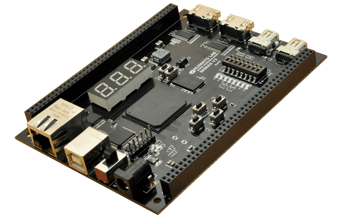
Designing a Gigabit Ethernet interface using an FPGA (Field-Programmable Gate Array) involves several steps, as the FPGA needs to manage both the high-speed transmission of data and the proper handling of Ethernet protocols. Here's a high-level guide to help you design a Gigabit Ethernet (1000BASE-T) interface on an FPGA.

1. Understand Gigabit Ethernet Standards (1000BASE-T)
- Physical Layer (PHY): Gigabit Ethernet uses the 1000BASE-T standard, which supports 1 Gbps speeds over twisted-pair copper cables (Cat 5e and above). The physical layer defines how data is encoded and transmitted.
- Encoding Scheme: 8b/10b encoding or PAM-5 (Pulse Amplitude Modulation 5-level) encoding is used for 1000BASE-T to ensure signal integrity over the transmission medium.
- Ethernet Frame Structure: The Ethernet frame format is specified by IEEE 802.3. Each Ethernet frame includes a preamble, start of frame delimiter (SFD), destination and source MAC addresses, payload, and CRC.
2. Key Components of a Gigabit Ethernet Design
- Ethernet MAC (Media Access Control): This layer handles the framing of data packets, addressing, and CRC calculation for error detection.
- Ethernet PHY (Physical Layer): This is responsible for the physical transmission and reception of data. The PHY converts the digital signals from the FPGA into analog signals for transmission over the network cable.
- FPGA: The FPGA will implement the MAC layer logic, control the PHY, and handle packet generation, transmission, and reception.
3. Selecting the Components
- FPGA Selection: Choose an FPGA with sufficient I/O pins, high-speed transceivers, and internal resources (logic cells, memory) to handle Gigabit Ethernet speeds. Popular choices are:
- Ethernet PHY Chip: You can use a standalone Gigabit Ethernet PHY chip like:
- RTL8201 (Realtek)
- KSZ9031 (Microchip)
- DP83867 (Texas Instruments)
- Ethernet MAC IP: If you’re using an FPGA from a major vendor like Xilinx or Intel, you can often use pre-designed MAC IP cores available in their development environments (e.g., Xilinx Vivado or Intel Quartus).
4. Design Steps
4.1. Create the Ethernet MAC Layer
The MAC layer is responsible for the following tasks:
- Frame Creation: Packets are framed with the destination and source MAC addresses, length/type fields, data, and CRC.
- Error Checking: The MAC layer adds a CRC (Cyclic Redundancy Check) to ensure data integrity.
- Flow Control: It manages packet flow and prevents buffer overflow by controlling data transmission rates.
You can:
- Use an IP Core: Both Xilinx and Intel provide Gigabit Ethernet MAC IP cores in their design environments.
- Build Your Own MAC: If you want to design your own MAC, you’ll need to handle packet framing, CRC calculation, and communication with the PHY.
4.2. PHY Interface
- Serial Communication (MII/RGMII): The Ethernet PHY communicates with the FPGA using an interface like MII (Media Independent Interface) or RGMII (Reduced Gigabit Media Independent Interface).
- MII: Standard 4-bit interface used for lower-speed Ethernet (10/100 Mbps).
- RMII: Simplified 2-bit interface for lower power consumption.
- RGMII: High-speed interface for Gigabit Ethernet.
- Clocking: Gigabit Ethernet PHY chips require an external clock (typically 125 MHz) to operate. Ensure that your FPGA is able to provide the required clock to the PHY or use an external oscillator.
4.3. Packet Transmission and Reception
- Transmitter: The FPGA must manage data buffers for outgoing packets and hand off the data to the PHY for transmission.
- Receiver: The FPGA needs to receive incoming data, perform error-checking (e.g., by verifying the CRC), and then forward the data to higher layers in the system.
4.4. Handle Timing and Synchronization
Gigabit Ethernet requires precise timing, including:
- Clock Domain Crossing: Data may need to be transferred between different clock domains (e.g., between the MAC and PHY), so careful management of clock domains is needed.
- TX and RX Synchronization: You must ensure that data transmitted and received is synchronized with the clock signals used by the PHY.
5. Designing the FPGA Logic
- State Machines: Use state machines to manage the transmission and reception of data. Typical states might include:
- Idle: Waiting for data to transmit or receive.
- Transmit: Sending data to the PHY.
- Receive: Receiving data from the PHY.
- Error Checking: Verifying CRC, handling frame errors.
- FIFO Buffers: Use FIFO buffers to store data temporarily as it’s transferred between the FPGA and the PHY. This helps manage data flow between the high-speed PHY and the lower-speed FPGA logic.
- Flow Control: Implement flow control mechanisms such as backpressure when the FPGA is unable to keep up with the incoming data rate.
6. Simulate the Design
- Simulation Tools: Use simulation tools like ModelSim, Vivado Simulator, or Quartus Simulator to validate your design.
- Testbenches: Write testbenches to simulate packet transmission and reception, check for correct timing, and verify that the PHY interface is working correctly.
7. Integrate the PHY and FPGA
Once your FPGA design is complete:
- Connect the FPGA to the PHY: Ensure that all necessary signals (TX, RX, MDI/MDX, etc.) are connected correctly between the FPGA and the PHY.
- Clocking: Ensure that the external clock for the PHY is supplied correctly.
- Verify the Interface: Use test equipment like an Ethernet analyzer to verify that data is transmitted and received correctly.
8. Real-Time Testing
After simulation, test the system with real Ethernet networks:
- Ethernet Switch: Connect the FPGA-based Ethernet interface to a standard Ethernet switch to test the connectivity and performance.
- Traffic Generation: Use traffic generators or software like iperf to generate network traffic and measure the throughput and latency of your design.
9. Optimization
- Performance: Ensure that the design can achieve full Gigabit speed (1 Gbps) under real-world conditions.
- Resource Utilization: Optimize the design to fit within the available FPGA resources (logic cells, memory, etc.). Use tools like Xilinx Vivado or Intel Quartus to analyze resource utilization and timing.
10. Possible Extensions
- Jumbo Frames: Support for larger-than-standard Ethernet frames can improve performance for certain types of traffic.
- VLAN Support: If required, add support for Ethernet Virtual LAN (VLAN) tagging to manage network traffic.
- Advanced Features: Depending on your application, consider adding features such as TCP/IP offload, Quality of Service (QoS), or flow control.
Example Block Diagram of the Design:
lua

+-------------------+   125 MHz   +-------------------+
| Ethernet MAC  | <--------->     |  Gigabit Ethernet |
|(FPGA Logic)   |   RGMII    |      PHY    |
+-------------------+          +-------------------+
  |   TX/RX  |           | TX/RX
  |        |            |
  +---------------+                |
  |        |            |
  |        |           |
   Ethernet Frames   Clock, Flow Control
Conclusion
Designing a Gigabit Ethernet interface based on FPGA is a complex but highly rewarding task. The key steps are selecting the right components (FPGA, PHY), designing the MAC logic, ensuring proper data synchronization and timing, and testing both in simulation and real hardware. By leveraging FPGA resources and Ethernet IP cores, you can build a robust, high-speed Ethernet interface suitable for a wide range of applications.
