Designing a USB 2.0 interface based on an FPGA (Field-Programmable Gate Array) involves creating the necessary logic to handle USB communication protocols, including data transmission, power management, and device enumeration. An FPGA can be used to implement both the USB host and device functionality, or just one of them, depending on your design requirements.
Here's an overview of the key steps involved in designing a USB 2.0 interface on an FPGA:
1. Understanding USB 2.0 Protocol
The USB 2.0 protocol consists of several layers of communication:
- Physical Layer (PHY): Defines the electrical characteristics, signaling, and data rates (High-Speed USB up to 480 Mbps, Full-Speed 12 Mbps, Low-Speed 1.5 Mbps).
- Data Link Layer: Responsible for packet framing, error detection, and flow control.
- Transaction Layer: Handles the higher-level management of packets and data transfer types (control, bulk, interrupt, isochronous).
- Application Layer: Defines how the data is interpreted by the device or host.
2. Choose USB 2.0 Role (Host or Device)
- Host: Controls the communication and provides power to the device. A USB host on FPGA typically requires more logic since it manages enumeration, power management, and control of multiple devices.
- Device: Responds to host requests. It typically requires simpler logic than the host since it only needs to respond to commands and transfer data.
You can choose to implement either a USB device (e.g., USB peripheral) or a USB host (e.g., USB controller), or both, depending on your application.
3. Key Components of USB 2.0 FPGA Design
USB PHY (Physical Layer Interface)
- The USB PHY is responsible for transmitting and receiving the data signals on the USB bus. Most FPGA manufacturers offer an external USB PHY that connects to the FPGA over a standard interface (e.g., SPI or parallel).
- Alternatively, you can design a custom PHY for USB 2.0, but this is more complex and generally not recommended unless you have specific requirements.
Data Link Layer (DLL)
- Packet Framing: The USB 2.0 data link layer handles the framing of packets into valid USB frames (e.g., Token, Data, and Handshake packets).
- Error Checking: This includes CRC checks to ensure the integrity of the transmitted data and automatic retransmission if errors occur.
Transaction Layer (TL)
- The transaction layer is responsible for managing higher-level communication, including the types of transfers:
- Control Transfers: Used for device management and configuration.
- Bulk Transfers: For transferring large amounts of data.
- Interrupt Transfers: For low-latency communication (e.g., mouse or keyboard).
- Isochronous Transfers: For time-sensitive data (e.g., audio or video).
- The TL includes managing the USB endpoint descriptors, packet handling, and coordination between different transfer types.
4. Implementing USB 2.0 on FPGA
Step 1: Set Up FPGA Development Environment
- Select a suitable FPGA development platform (e.g., Xilinx, Intel/Altera, Lattice).
- Set up a hardware description language (HDL) environment using VHDL or Verilog.
- Use FPGA development tools (e.g., Vivado for Xilinx or Quartus for Intel FPGAs) to compile and synthesize the design.
Step 2: USB 2.0 Core
- USB Core: You can either implement your own USB 2.0 core from scratch or use a pre-existing USB 2.0 IP core. Many FPGA vendors provide USB 2.0 cores that implement the USB data link and transaction layers.
- Xilinx offers a USB 2.0 Device/Host Controller IP core.
- Intel/Altera provides USB 2.0 PHY cores and controller solutions.
- These cores typically include support for the physical layer, data link layer, and transaction layer, making it easier to focus on the application layer.
Step 3: USB Transceiver/PHY
- For USB 2.0 high-speed operation (480 Mbps), you’ll need to integrate a USB transceiver (PHY) to handle the physical layer signaling. This transceiver connects to the FPGA’s logic, providing USB signal driving and receiving functions.
- USB 2.0 PHYs often come as external chips or as part of an IP core in FPGA development kits.
Step 4: Implementing USB Data Transfer Logic
- Depending on whether you're designing a USB device or USB host, the logic will handle the different types of transfers (Control, Bulk, Interrupt, Isochronous).
- For USB devices, you'll need to implement endpoint buffers, handle requests from the host (such as GET DESCRIPTOR, SET CONFIGURATION), and manage data flow.
- For USB hosts, you need logic to enumerate devices, handle hub control, and manage data transfers with connected devices.
Step 5: Interface with Application Logic
- The USB transaction layer interacts with the application layer, where the data will be used. For example, if the FPGA is acting as a USB mass storage device, you will need to implement a storage controller (e.g., SD card or Flash memory interface) that communicates via USB.
- For a USB host, you may need to handle peripheral device communication, like reading data from a connected USB device.
5. Debugging and Testing
- USB communication requires careful testing of both the hardware (electrical signals) and the protocol (correct implementation of transfers).
- Logic Analyzers can be used to capture and decode USB traffic for debugging purposes.
- Use FPGA simulation tools to test the functionality of the design at the HDL level before programming the FPGA.
6. Example FPGA USB Designs
Here are some examples of how USB 2.0 can be implemented in FPGA-based systems:
- USB Device: An FPGA can be programmed to behave as a USB device, such as a USB-to-SPI bridge, mass storage device, or a custom HID (Human Interface Device) like a mouse or keyboard.
- USB Host: An FPGA can act as a USB host controller to interface with USB peripherals like mice, keyboards, storage devices, or sensors.
7. Recommended Tools and Resources
- USB 2.0 IP Cores: Prebuilt IP cores are available from FPGA vendors, and third-party vendors like Microchip, Lattice, and DesignWare.
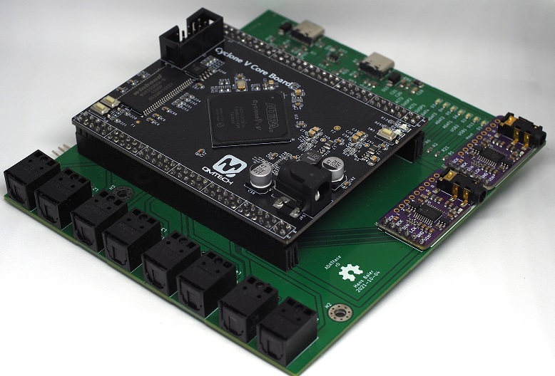
- FPGA Development Kits: Many FPGA kits include integrated USB support and allow you to test the USB interface easily (e.g., Xilinx Spartan-6, Intel Cyclone V).
- USB Protocol Analyzers: Tools like Total Phase USB Analyzer or software-based USB analyzers (e.g., Wireshark with USB packet decoding) can help debug USB traffic.
Conclusion
Designing a USB 2.0 interface based on FPGA involves using FPGA logic to implement both the low-level physical interface (PHY) and higher-level communication protocols (transaction layer). You can leverage pre-built cores for USB functionality, and the design complexity will vary depending on whether you're implementing a host or device. The FPGA’s flexibility allows for custom and high-performance solutions in USB applications, but careful attention to detail is required for effective data transfer and protocol compliance.
