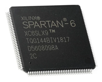
An example of a high-capacity, low-cost FPGA is the Spartan 6 series. It uses low-power copper-clad 45nm technology, which can balance cost, performance, and power consumption. The Spartan 6 series employs dual-register, six-input LUTs and one Series of built-in system-level modules, including the 18Kb Block Ram, second-generation DSP48A21 Slice, SDRAM memory interface (DDR interface), robust hybrid clock management module, Select IO technology, and optimized high-speed serial transceiver GTP Transceiver, PCIe interface, advanced system-level power management mode, automatic configuration detection, and enhanced IP with AES and Dev. Spartan 6 excels at user-centric DSP design, low-cost logic design, and high-capacity logic design.
Feature
Low design cost
Low dynamic and static power consumption
45nm technology has optimized power consumption;
Zero power consumption in sleep mode;
In the suspend mode, the internal state of the chip can be maintained, and there are multiple pins to realize the wake-up operation of the chip;
LX FPGAs, -1L uses a core voltage of 1.0V; LX and LXT FPGAs, -2, -3, and -3N uses a core voltage of 1.2V;
Select IO can adopt multi-level standards
Each pair of differential IO can reach a data transmission speed of up to 1080Mb/s;
The output current of each pin is up to 24mA;
1.2--3.3V level standards and protocols for selection;
Low-power HSTL, SSTL memory interface technology;
Comply with hot-swap specification;
Adjustable IO interface chip slope to improve signal integrity;
High-speed serial transceiver (only available in LXT FPGA);
Supported high-speed interfaces include Serial ATA, Aurora, 1G Ethernet, PCI Express, OBSAI, CPRI, EPON, GPON, DisplayPort, and XAUI;
Endpoint block used in PCIe interface design (LXT FPGA only)
Support PCI interface, compatible with 33MHZ, 32bit/64bitPCI protocol
Efficient DSP48A1 module
Fast 18X18 multiplier or 48bit accumulator, with the ability to stream and cascade;
Integrated memory control interface module
Support DDR, DDR2, DDR3 and LPDDR;
The data rate is up to 800Mb/s;
The memory control interface has multiple ports, each port contains its own independent FIFO, which can realize high-speed reading and writing of the memory;
Sufficient logical resources
Optional shift register or distributed RAM;
Efficient 6-input LUT;
Block RAM
Each block RAM is 18Kb in size, and one block RAM can be used as two 9Kb block RAMs through programming;
Clock Management Tile (CMT) clock management module
16 low-skew clock networks; internal DCM can eliminate clock skew and cycle distortion changes; internal PLL can achieve phase lock and achieve low clock jitter;
Simplified device configuration
There are two pins for automatic detection of configuration mode;
Support SPI Flash (up to 4) and Nor Flash configuration;
Xilinx Platform Flash programmed with JTAG;
Support multi-boot to facilitate remote upgrade;
The unique Device DNA logo is used for design certification;
AES bitstream encryption;
Support MicroBlaze soft processor system
Rich industrial IP and reference designs
Application
Car infotainment
Flat panel display
Video Surveillance