Time: 2025-02-20 11:08:54View:
Field-Programmable Gate Arrays (FPGAs) are highly versatile integrated circuits that can be configured by the user to implement custom digital logic designs. Understanding their internal structure is crucial for effectively utilizing them in hardware design. Here's a detailed breakdown of what you need to know about the internal structure of FPGAs:
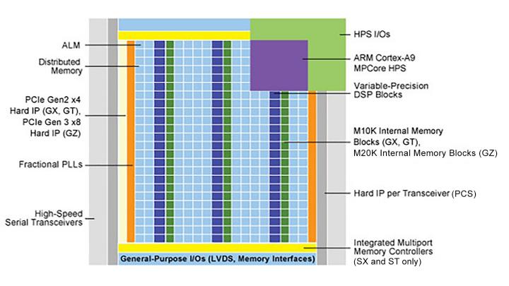
1. Configurable Logic Blocks (CLBs):
CLBs are the fundamental building blocks of an FPGA.
Each CLB consists of Look-Up Tables (LUTs), flip-flops, and multiplexers.
LUTs: Implement combinational logic by storing truth tables.
Flip-Flops: Store state information for sequential logic.
CLBs can be configured to perform basic logic operations (AND, OR, XOR, etc.) or more complex functions.
2. Programmable Interconnects:
These are the routing resources that connect CLBs and other components.
Interconnects are made up of wires and programmable switches.
They allow for flexible routing of signals between logic blocks.
3. Input/Output Blocks (IOBs):
IOBs provide the interface between the FPGA and external devices.
They can be configured as input, output, or bidirectional pins.
Support various voltage standards (e.g., LVDS, LVCMOS).
4. Block RAM (BRAM):
Dedicated memory blocks for storing data.
Can be configured as single-port or dual-port RAM.
Used for implementing memory-intensive applications like buffers or FIFOs.
5. DSP Slices:
Specialized blocks for performing arithmetic operations like multiplication, addition, and accumulation.
Ideal for digital signal processing (DSP) applications.
6. Clock Management Resources:
Includes Phase-Locked Loops (PLLs) and Delay-Locked Loops (DLLs).
Used for clock signal generation, frequency synthesis, and clock domain management.
7. Specialized Hard IP Cores:
Pre-designed blocks for specific functions like PCIe, Ethernet, or memory controllers.
These cores are optimized for performance and reduce the need for custom logic.
FPGAs are organized in a hierarchical manner, with CLBs grouped into larger structures called tiles or slices.
These tiles are interconnected through a global routing network.
2. Configuration Memory:
FPGAs use SRAM-based configuration memory to store the user's design.
The configuration is loaded at startup and can be reprogrammed as needed.
3. Partial Reconfiguration:
Some FPGAs support partial reconfiguration, allowing specific parts of the device to be reconfigured while the rest remains operational.
1. Design Entry:
The user describes the desired logic using Hardware Description Languages (HDLs) like VHDL or Verilog.
Alternatively, high-level synthesis (HLS) tools can be used to generate HDL from C/C++ or Python.
2. Synthesis:
The HDL code is synthesized into a netlist, which represents the logic design in terms of FPGA primitives (LUTs, flip-flops, etc.).
3. Place and Route:
The netlist is mapped onto the FPGA's physical resources (CLBs, DSP slices, etc.).
The place-and-route tool determines the optimal placement of logic blocks and routing paths.
4. Configuration:
The final design is converted into a bitstream, which is loaded into the FPGA's configuration memory.
The FPGA then operates according to the user's design.
FPGAs can be reprogrammed to implement virtually any digital circuit.
2. Parallelism:
FPGAs can perform multiple operations simultaneously, making them ideal for high-performance applications.
3. Customizability:
Users can optimize the design for specific requirements, such as power, speed, or area.
1. Complexity:
Designing for FPGAs requires expertise in digital logic and hardware description languages.
2. Resource Constraints:
Limited CLBs, DSP slices, and BRAMs require careful resource management.
3. Timing Closure:
Ensuring that signals meet timing requirements can be challenging, especially in high-speed designs.
1. Digital Signal Processing:
FPGAs are widely used in applications like audio/video processing, radar, and wireless communication.
2. Prototyping and Emulation:
FPGAs are used to prototype ASIC designs before fabrication.
3. High-Performance Computing:
FPGAs accelerate tasks like machine learning, cryptography, and data analytics.
4. Industrial Automation:
Used in motor control, robotics, and real-time control systems.
2. Intel (formerly Altera):
Focuses on low-power FPGAs.
4. Microchip (formerly Microsemi):
Known for radiation-tolerant FPGAs for aerospace applications.
By understanding the internal structure of FPGAs, you can leverage their flexibility and performance to create custom hardware solutions tailored to your specific needs.
