Time: 2025-02-26 11:09:23View:
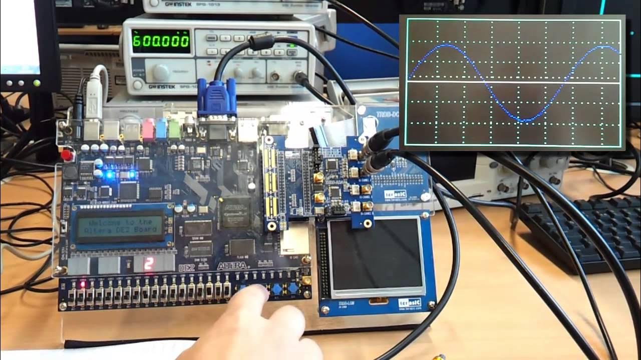
Objective: To design a digital oscilloscope using a Field-Programmable Gate Array (FPGA) for signal acquisition, processing, and display.
Scope: The oscilloscope will capture analog signals, digitize them, process the data, and display the waveform on a screen. The FPGA will handle real-time signal processing and control.
Functional Requirements:
Capture analog signals with a specified bandwidth (e.g., 100 MHz).
Digitize the signal using an Analog-to-Digital Converter (ADC).
Process and store the digitized signal in real-time.
Display the waveform on a screen (e.g., VGA or LCD).
Provide user controls for timebase, voltage scaling, and triggering.
Non-Functional Requirements:
High-speed signal processing.
Low latency and high accuracy.
User-friendly interface.
Scalability for higher bandwidths or additional features.
Hardware Components:
FPGA: e.g., Xilinx Spartan or Altera Cyclone series.
Analog Front-End: Signal conditioning (amplification, attenuation, filtering).
ADC: High-speed ADC (e.g., 8-bit, 100 MSPS).
Memory: SRAM or SDRAM for storing sampled data.
Display Interface: VGA or LCD for waveform visualization.
User Input: Buttons, knobs, or touchscreen for control.
Clock Generator: For synchronizing ADC and FPGA operations.
Software Components:
FPGA Firmware: Written in VHDL or Verilog for signal acquisition, processing, and control.
Signal Processing Algorithms: For filtering, triggering, and scaling.
Display Driver: To render waveforms on the screen.
User Interface Logic: To handle user inputs and adjust settings.
Block Diagram:
+-------------------+       +-------------------+       +-------------------+
|   Analog Front-End|       |   ADC             |       |   Clock Generator |
+-------------------+       +-------------------+       +-------------------+
        |                         |                         |
        v                         v                         v
+---------------------------------------------------------------+
|                      FPGA                                     |
|                                                               |
|  +-------------------+       +-------------------+             |
|  | Signal Acquisition|       | Signal Processing |             |
|  | & Control         |       | & Storage         |             |
|  +-------------------+       +-------------------+             |
|                                                               |
+---------------------------------------------------------------+
        |                         |                         |
        v                         v                         v
+-------------------+       +-------------------+       +-------------------+
|   Memory          |       |   Display Driver  |       |   User Interface  |
+-------------------+       +-------------------+       +-------------------+
        |                         |
        v                         v
+-------------------+       +-------------------+
|   SRAM/SDRAM      |       |   VGA/LCD Display |
+-------------------+       +-------------------+
Hardware Implementation:
Design the analog front-end to condition the input signal (amplification, filtering).
Connect the ADC to the FPGA for digitizing the signal.
Interface the FPGA with memory (SRAM/SDRAM) for storing sampled data.
Connect the FPGA to a VGA or LCD display for waveform visualization.
Provide user input controls (buttons, knobs, or touchscreen).
FPGA Firmware Implementation:
Signal Acquisition:
Implement logic to control the ADC and capture data at the desired sampling rate.
Signal Processing:
Apply digital filters (e.g., FIR/IIR) for noise reduction.
Implement triggering logic (e.g., edge, pulse, or level triggering).
Scale the data for voltage and timebase adjustments.
Display Driver:
Render the waveform on the screen using VGA or LCD protocols.
User Interface:
Handle user inputs to adjust settings (e.g., timebase, voltage scaling, trigger type).
Code Snippets:
-- Example: ADC Interfaceprocess(clk)begin
    if rising_edge(clk) then
        if adc_ready = '1' then
            sampled_data <= adc_data;
            store_data(sampled_data);
        end if;
    end if;end process;-- Example: Triggering Logicprocess(sampled_data)begin
    if sampled_data > trigger_level and trigger_enabled = '1' then
        trigger_event <= '1';
    else
        trigger_event <= '0';
    end if;end process;
Unit Testing: Test individual modules (ADC interface, signal processing, display driver).
Integration Testing: Verify the interaction between modules.
Performance Testing: Measure the system's bandwidth, accuracy, and latency.
User Testing: Ensure the interface is intuitive and responsive.
The FPGA-based oscilloscope provides a flexible and high-performance solution for signal analysis.
Future enhancements could include additional measurement features (e.g., FFT, protocol decoding), higher bandwidth, or network connectivity.
FPGA datasheets and development tools (e.g., Xilinx Vivado, Intel Quartus).
ADC and memory component datasheets.
Relevant literature on digital oscilloscope design and FPGA-based systems.
This outline provides a comprehensive approach to designing an oscilloscope using an FPGA. The actual implementation details will depend on the specific components and requirements of the project.
