Time: 2025-03-10 11:45:59View:
Implementing SDI (Serial Digital Interface) video encoding and decoding using a Kintex-7 series FPGA is a robust solution for high-speed video processing applications. The Kintex-7 FPGA, part of Xilinx's 7th-generation FPGAs, offers high-performance logic, DSP slices, and high-speed serial transceivers, making it well-suited for SDI video processing. Below is a detailed guide on how to implement SDI video encoding and decoding using the Kintex-7 FPGA.
SDI is a standard for transmitting uncompressed digital video over coaxial cables. Common SDI standards include:
SD-SDI: Standard Definition (270 Mbps)
HD-SDI: High Definition (1.485 Gbps)
3G-SDI: 3Gbps for higher resolutions (e.g., 1080p60)
6G-SDI and 12G-SDI: For 4K and 8K video.
The Kintex-7 FPGA supports these standards through its high-speed GTX transceivers.
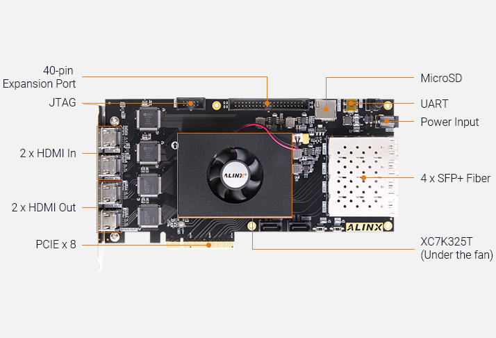
Kintex-7 FPGA: Choose a device with sufficient GTX transceivers (e.g., XC7K325T or XC7K410T).
SDI Interface: Coaxial connectors and cables compatible with SDI standards.
Video Source and Sink: Cameras, monitors, or other SDI-compatible devices.
Memory: DDR3 or DDR4 for buffering video frames (if needed).
Clock Management: High-precision clock generators for SDI timing.
Xilinx Vivado Design Suite: For FPGA design, synthesis, and implementation.
SDI IP Cores: Xilinx provides SDI IP cores for encoding and decoding.
Simulation Tools: For testing and verification (e.g., ModelSim).
Define the SDI standard to be implemented (e.g., HD-SDI or 3G-SDI).
Plan the video pipeline: encoding, decoding, and any additional processing (e.g., scaling, color space conversion).
Allocate FPGA resources (e.g., GTX transceivers, DSP slices, and block RAM).
Open Xilinx Vivado and create a new project targeting the Kintex-7 FPGA.
Add the necessary IP cores for SDI encoding and decoding.
Use Xilinx's SDI IP Core for encoding and decoding.
SDI Transmitter (TX): Converts parallel video data into serial SDI output.
SDI Receiver (RX): Converts serial SDI input into parallel video data.
Configure the IP cores for the desired SDI standard (e.g., HD-SDI or 3G-SDI).
Set the GTX transceiver parameters (e.g., line rate, reference clock).
Encoding:
Input: Parallel video data (e.g., from a camera or memory).
Process: Apply video processing (e.g., color space conversion, scaling).
Output: Serial SDI data via the GTX transceiver.
Decoding:
Input: Serial SDI data from the GTX transceiver.
Process: Convert to parallel video data and apply any required processing.
Output: Parallel video data for display or further processing.
Use Xilinx's Clock Management Wizard to generate the required clocks for SDI timing.
Ensure proper synchronization between the video source, FPGA, and display.
Synthesize and implement the design in Vivado.
Program the FPGA and test with real SDI video sources and sinks.
Use debugging tools (e.g., ILA - Integrated Logic Analyzer) to verify signal integrity.
The Kintex-7 FPGA's GTX transceivers are used for high-speed serial communication.
Configure the transceivers to match the SDI line rate (e.g., 1.485 Gbps for HD-SDI).
Xilinx provides a dedicated SDI IP core for encoding and decoding.
The IP core handles the SDI protocol, including line and frame synchronization.
Use FPGA logic and DSP slices for video processing tasks (e.g., color space conversion, scaling).
Implement custom logic or use Xilinx's Video Processing Subsystem IP for advanced processing.
Input: Receive parallel video data (e.g., 8-bit or 10-bit YCbCr).
Encoding:
Process the video data (if needed).
Use the SDI TX IP core to serialize the data and output it via the GTX transceiver.
Transmission: Send the serial SDI data over a coaxial cable.
Decoding:
Receive the serial SDI data via the GTX transceiver.
Use the SDI RX IP core to deserialize the data into parallel video data.
Output: Send the parallel video data to a display or further processing.
Signal Integrity: Ensure proper PCB design and impedance matching for SDI signals.
Timing Constraints: Use Vivado's timing analysis tools to meet SDI timing requirements.
Resource Utilization: Optimize FPGA resource usage by leveraging DSP slices and block RAM.
Xilinx Vivado: For FPGA design and implementation.
SDI IP Core Documentation: Available in Xilinx's documentation.
Reference Designs: Xilinx provides example designs for SDI applications.
Simulation Tools: Use ModelSim or Vivado's built-in simulator for testing.
// Pseudocode for SDI encoding and decodingmodule sdi_top (
    input  wire clk,          // System clock
    input  wire reset,        // System reset
    input  wire [9:0] video_in, // Parallel video input
    output wire sdi_tx,       // Serial SDI output
    input  wire sdi_rx,       // Serial SDI input
    output wire [9:0] video_out // Parallel video output);

    // SDI Transmitter
    sdi_tx_ip sdi_tx_inst (
        .clk(clk),
        .reset(reset),
        .video_in(video_in),
        .sdi_tx(sdi_tx)
    );

    // SDI Receiver
    sdi_rx_ip sdi_rx_inst (
        .clk(clk),
        .reset(reset),
        .sdi_rx(sdi_rx),
        .video_out(video_out)
    );endmodule
Using the Kintex-7 FPGA for SDI video encoding and decoding is a powerful solution for professional video applications. By leveraging Xilinx's SDI IP cores and the FPGA's high-speed GTX transceivers, you can implement a robust and efficient SDI video processing system. Ensure proper design, testing, and optimization to meet the stringent requirements of SDI standards.
