Time: 2025-04-07 11:20:39View:
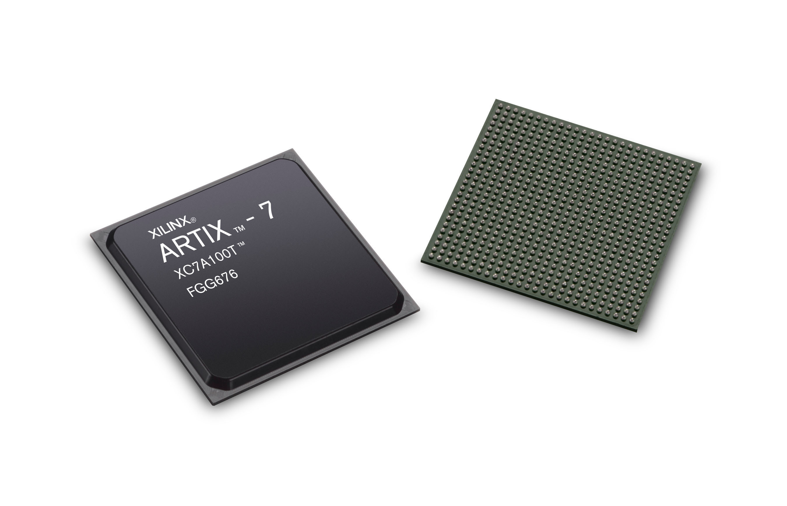
Xilinx 7 Series FPGAs (including Artix-7, Kintex-7, and Virtex-7) provide highly optimized on-chip storage resources, making them ideal for applications requiring high-speed data buffering, lookup tables, and memory-intensive processing. Below are the key advantages of their storage architecture.

✔ 36 Kb (or 18 Kb) dedicated memory blocks per BRAM.
✔ True Dual-Port (TDP) support – Independent read/write on both ports.
✔ Configurable widths (×1, ×2, ×4, ×9, ×18, ×36).
✔ Synchronous operation with optional pipeline registers for high-speed designs.
✔ ECC (Error Correction Code) support (in UltraScale+ and selected 7 Series).
✅ Low-latency access (1-2 clock cycles).
✅ No external memory needed for small-to-medium datasets.
✅ Flexible usage (FIFOs, ROMs, register files, data buffers).
Example: A Virtex-7 XC7VX690T has 1,470 BRAMs (53 Mb total).
✔ Built using LUTs (Look-Up Tables) in SLICEM (memory-capable slices).
✔ Supports small, fast memories (up to 64×1 or 32×2 per LUT).
✔ Single-port or simple dual-port modes.
✅ Ultra-low latency (1 cycle).
✅ Efficient for small storage needs (e.g., shift registers, coefficient storage).
✅ Does not consume BRAM resources.
Example: Implementing a 32×8-bit register file using 8 LUTs in SLICEM.
(Note: 7 Series does not have URAM, but its BRAM is highly optimized for similar use cases.)
Feature | BRAM (7 Series) | URAM (UltraScale+) |
Capacity | 36 Kb per block | 288 Kb per block |
Ports | Dual-port | Dual-port |
ECC | Limited support | Full ECC support |
Best For | Medium storage | Large buffers |
Workaround in 7 Series: Cascading BRAMs for larger memory needs.
✔ Implemented using LUTs in SRL mode (up to 32-bit shift depth).
✔ No extra logic needed for serial-in, serial-out (SISO) buffers.
✅ Saves flip-flops compared to manual shift registers.
✅ Low power & compact for small delay lines.
Example: A 16-tap delay line using one LUT (SRL16E).
✔ Xilinx FIFO Generator IP supports:
l Synchronous/Asynchronous clocks.
l Standard or AXI4-Stream interfaces.
l Programmable almost-full/empty flags.
✅ Seamless integration with Xilinx IP cores.
✅ Configurable for different data widths/depths.
Example: A 512×32-bit FIFO for UART buffering.
✔ 7 Series FPGAs load configuration from:
l SPI Flash (external).
l BPI (Parallel NOR Flash).
l JTAG/USB programming.
✔ eFUSE & AES encryption for secure bitstream storage.
✅ Persistent configuration after power-off.
✅ Supports secure boot.
Feature | Xilinx 7 Series | Intel Cyclone 10 |
BRAM Size | 36 Kb per block | 20 Kb (M20K) |
Distributed RAM | LUT-based | MLAB (640 bits) |
ECC Support | Limited (UltraScale+ full) | Yes |
FIFO Support | Built-in IP | Built-in IP |
✅ Xilinx 7 Series wins in BRAM capacity & flexibility.
Storage Type | Use Case |
BRAM | Packet buffering, image processing |
Distributed RAM | Small LUTs, coefficient storage |
SRL Shift Registers | Delay lines, small FIFOs |
FIFO Generator | Data synchronization across clock domains |
The Xilinx 7 Series FPGAs provide exceptional on-chip storage with:
✔ High-density BRAM (up to 53 Mb in Virtex-7).
✔ Flexible distributed RAM (LUT-based).
✔ Efficient shift registers (SRL).
✔ Reliable FIFO & configuration memory.
For high-performance designs, the 7 Series remains competitive against newer FPGAs due to its optimized BRAM architecture.