Time: 2025-04-24 11:38:40View:
Implementing an ADC (Analog-to-Digital Converter) on an FPGA requires careful consideration of the ADC type, interface, and digital logic design. Below is a structured guide to help you integrate an ADC with an FPGA (e.g., Xilinx, Intel/Altera, or Lattice).
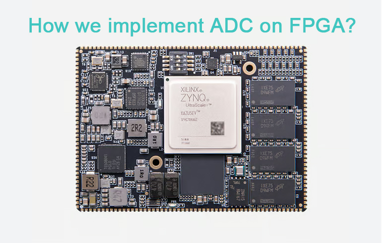
FPGAs typically interface with external ADCs, but some include on-chip ADCs (e.g., Xilinx Zynq Ultrascale+ or Intel MAX 10). Common ADC types:
| ADC Type | Resolution | Speed | Interface | Use Case |
|---|---|---|---|---|
| SAR (Successive Approximation) | 8-16 bits | Slow (1 MSPS) | SPI, I2C, Parallel | Low-power, general-purpose |
| Sigma-Delta (ΔΣ) | 16-24 bits | Slow (kHz range) | SPI | High-precision (audio, sensors) |
| Pipeline ADC | 8-14 bits | Fast (10+ MSPS) | LVDS, JESD204B | High-speed (video, RF) |
| Flash ADC | 6-10 bits | Ultra-fast (1+ GSPS) | Parallel | Ultra-high-speed (radar, SDR) |
| Interface | FPGA Pins Used | Pros | Cons |
|---|---|---|---|
| SPI | 3-4 (SCLK, MOSI, MISO, CS) | Simple, low pin count | Slow (~1-10 MHz) |
| I2C | 2 (SCL, SDA) | Low pin count | Slower (~400 kHz) |
| Parallel | 8-16+ (data bus + control) | Fast (no protocol overhead) | High pin count |
| LVDS/JESD204B | Differential pairs | Ultra-high-speed (GSPS) | Complex, needs SERDES |
| ADC Pin | FPGA Pin | Description |
|---|---|---|
| VREF | 3.3V | Reference voltage |
| CLK | FPGA GPIO | SPI clock (SCLK) |
| DIN | FPGA GPIO | MOSI (commands) |
| DOUT | FPGA GPIO | MISO (ADC data) |
| CS | FPGA GPIO | Chip select |
module spi_adc (
    input wire clk,         // FPGA clock (e.g., 50 MHz)
    input wire start,       // Start conversion
    output reg [11:0] data, // 12-bit ADC result
    output reg busy,        // Conversion in progress
    // SPI interface
    output wire sclk,
    output wire cs,
    output wire mosi,
    input wire miso);reg [3:0] bit_counter;reg [15:0] shift_reg; // For SPI data exchange// SPI clock generation (divide FPGA clock)reg [7:0] clk_div = 0;always @(posedge clk) begin
    clk_div <= clk_div + 1;endassign sclk = clk_div[3]; // SPI clock = clk/16 (~3.125 MHz @ 50 MHz FPGA)// State machinealways @(posedge clk) begin
    if (start && !busy) begin
        busy <= 1;
        bit_counter <= 0;
        shift_reg <= 16'h0600; // MCP3208 command: start bit + single-ended CH0
    end
    else if (busy) begin
        if (clk_div == 8'hFF) begin
            shift_reg <= {shift_reg[14:0], miso}; // Shift in ADC data
            bit_counter <= bit_counter + 1;
            if (bit_counter == 15) begin
                busy <= 0;
                data <= shift_reg[11:0]; // Store 12-bit result
            end
        end
endendassign cs = ~busy; // Active-low CSassign mosi = shift_reg[15]; // MSB firstendmodulemodule parallel_adc ( input wire clk, input wire [11:0] adc_data, // 12-bit parallel ADC input input wire adc_ready, // ADC data-ready strobe output reg [11:0] captured_data);always @(posedge clk) begin if (adc_ready) begin captured_data <= adc_data; // Latch ADC data endendendmodule
`timescale 1ns/1psmodule tb_spi_adc();reg clk = 0;reg start = 0;wire [11:0] data;wire busy, sclk, cs, mosi;reg miso = 0;spi_adc uut (clk, start, data, busy, sclk, cs, mosi, miso);always #10 clk = ~clk; // 50 MHz clockinitial begin
    // Simulate ADC response (MISO)
    #100 start = 1;
    #20 start = 0;

    // Simulate ADC sending 0xABC (12-bit)
    wait(busy);
    repeat(16) begin
        #160 miso = $random; // Random data for testing
    end
    $display("ADC Data: %h", data);
$finish;endendmoduleClock Domain Crossing (CDC)
If the ADC runs asynchronously, use FIFOs or synchronizers to avoid metastability.
Noise Reduction
Add decoupling capacitors near ADC power pins.
Use differential signaling (LVDS) for high-speed ADCs.
Calibration
Correct for offset/gain errors in FPGA logic (e.g., subtract DC bias).
FPGA-Specific Resources
Xilinx: Use IDDR/ODDR for LVDS.
Intel: Use LVDS buffers in Quartus.
Some FPGAs have built-in ADCs:
Xilinx Zynq: XADC (12-bit, 1 MSPS).
Intel MAX 10: 12-bit, 1 MSPS.
Example (Xilinx XADC):
// XADC instantiation (Xilinx)xadc_wiz_0 xadc (
    .daddr_in(6'h00), // Channel 0 (temp sensor)
    .dclk_in(clk),
    .den_in(1'b1),
    .do_out(adc_data));
Choose ADC type (SAR, Sigma-Delta, Pipeline).
Interface with FPGA (SPI, Parallel, LVDS).
Implement digital logic (Verilog/VHDL).
Simulate & verify (testbench).
Optimize for noise/speed (PCB + FPGA design).
