Time: 2025-05-06 11:12:34View:
FPGAs contain specialized clocking resources designed to manage and distribute clock signals efficiently throughout the device. Understanding these resources is crucial for proper FPGA design. Here's a detailed breakdown:
Purpose: Distribute clocks with minimal skew across the entire FPGA
Characteristics:
Low-skew, high-fanout networks
Typically 8-16 global lines per device
Can drive all synchronous elements (FFs, RAMs, DSPs)
Usage: Primary system clocks, high-speed interfaces
Purpose: Serve specific device regions with lower power consumption
Characteristics:
Shorter routes than global clocks
Lower skew within their region
Typically 4-8 per device quadrant
Usage: Clock domains for specific functional blocks
Purpose: Interface with external high-speed devices
Characteristics:
Special low-skew paths to I/O banks
Support high-speed serial interfaces
Usage: DDR memory interfaces, high-speed serial I/O
Functions:
Clock multiplication/division
Phase shifting
Jitter filtering
Clock deskewing
Typical Specs:
Input frequency range: 5-650MHz
Output frequency range: 1-800MHz
4-10 output taps per PLL
Advanced Features:
Fractional frequency synthesis
Fine-grained phase adjustment
Dynamic reconfiguration
Found in: Xilinx UltraScale/7-series devices
Primary Function: Clock deskewing
Characteristics:
Zero-delay buffering
Fixed or variable delay lines
                     +---------------+
                     |    PLL/MMCM   |
                     +-------┬-------+
                             |
              +--------------+--------------+
              |              |              |
        +-----v-----+  +-----v-----+  +-----v-----+
        | Global    |  | Regional |  | I/O Clock |
        | Clock Buf |  | Clock Buf|  |   Buf     |
        +-----┬-----+  +-----┬-----+  +-----┬-----+
              |              |              |
      +-------v-------+   +--v----------+  |
      | Core Logic    |   | Regional    |  |
      | (CLBs, DSP,   |   | Logic       |  |
      |  Block RAM)   |   +-------------+  |
      +---------------+                    |
                                           |
                                 +---------v---------+
                                 | High-Speed I/O    |
                                 | (SerDes, DDR)     |
                                 +-------------------+
Implementation: Gating through logic (preferred over physical gating)
Best Practice: Use synchronous clock enables rather than gated clocks
Types:
Glitch-free muxes (dedicated hardware)
Synchronized muxes (implemented in logic)
Types:
BUFG: Global clock buffer
BUFR: Regional clock buffer
BUFIO: I/O clock buffer
BUFH: Horizontal clock buffer (Xilinx specific)
For power management or performance scaling
Requires glitch-free switching circuits
Synchronizer cells
Dual-clock FIFOs
Pulse synchronizers
For low-speed clock distribution
Higher skew tolerance
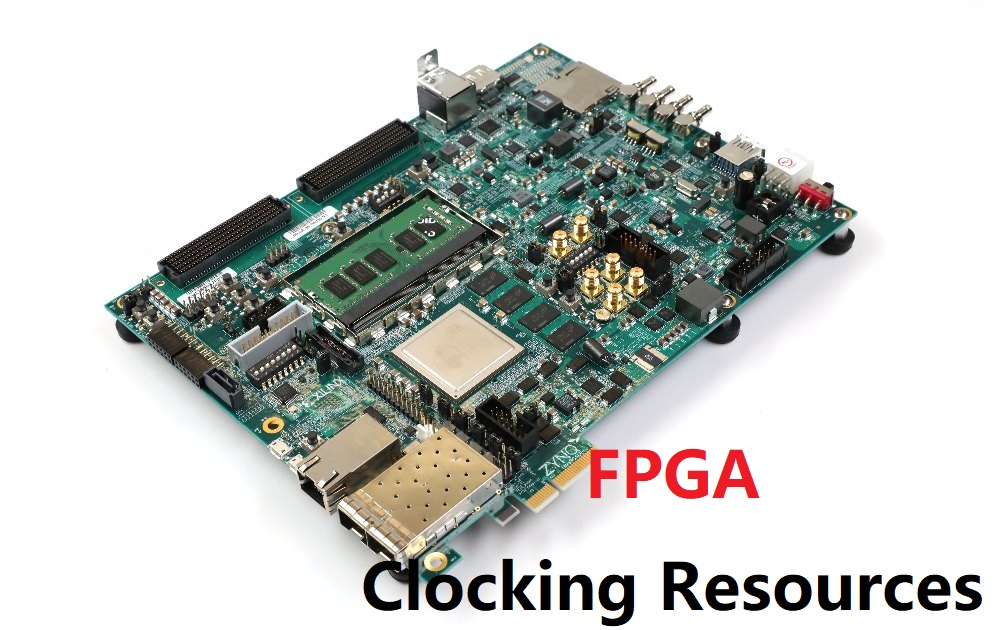
Your board features:
4 PLLs per FPGA device
16 global clock networks
8 dual-regional clock networks
Periphery clock networks for I/O banks
Hierarchical Clock Design:
// Good practice example
module top (
    input wire clk_100mhz,
    output wire [7:0] leds
);
    wire clk_50mhz;
    wire clk_locked;

    // PLL instantiation
    sys_pll pll_inst (
        .refclk(clk_100mhz),
        .rst(1'b0),
        .outclk_0(clk_50mhz),
        .locked(clk_locked)
    );

    // Clock domain module
    clock_50mhz_domain module_inst (
        .clk(clk_50mhz),
        .reset_n(clk_locked),
        .leds(leds)
    );
endmodule
Constraint Examples (SDC format):
# Primary clock definition
create_clock -name sys_clk -period 10 [get_ports clk_100mhz]

# Generated clock definition
create_generated_clock -name clk_50mhz \
    -source [get_pins pll_inst|altpll_component|pll|clk[0]] \
        -divide_by 2 \
            [get_pins pll_inst|altpll_component|pll|clk[1]]

            # Clock groups for asynchronous domains
            set_clock_groups -asynchronous -group {sys_clk} -group {clk_50mhz}
Implementation Tips:
Use dedicated clock routing whenever possible
Minimize the number of clock domains
Properly constrain all clocks
Verify clock domain crossings
Use vendor-specific clocking primitives
