Time: 2024-11-21 11:28:28View:
FPGAs (Field-Programmable Gate Arrays) are versatile devices used for digital logic design. The SLICE is the fundamental unit of computation within an FPGA, specifically part of the Configurable Logic Block (CLB). This article delves into the SLICE’s architecture, functionality, and how it plays a crucial role in FPGA designs.
An FPGA is an integrated circuit designed to be configured by the user after manufacturing, enabling custom logic functions. FPGAs are programmed using hardware description languages (HDLs) and can be reconfigured as needed, offering flexibility for a wide variety of applications.
The typical FPGA architecture includes:
Configurable Logic Blocks (CLBs) are the functional units of an FPGA that can be programmed to perform logical operations. A CLB contains multiple SLICEs, which are the building blocks that perform these operations. These logic blocks can implement a wide range of functions from simple logic gates to complex arithmetic.
| Component | Description |
|---|---|
| LUTs (Look-Up Tables) | Implement combinational logic functions. Each LUT can be programmed to perform different logic operations. |
| Flip-Flops | Store data and create sequential circuits, providing memory and state storage within CLBs. |
| Multiplexers | Route data through different parts of the FPGA, enabling flexible logic configurations. |
CLBs allow FPGAs to implement any digital logic function. By configuring the LUTs, flip-flops, and multiplexers, designers can create anything from a simple gate to a complex processing unit, such as a microprocessor or digital filter.
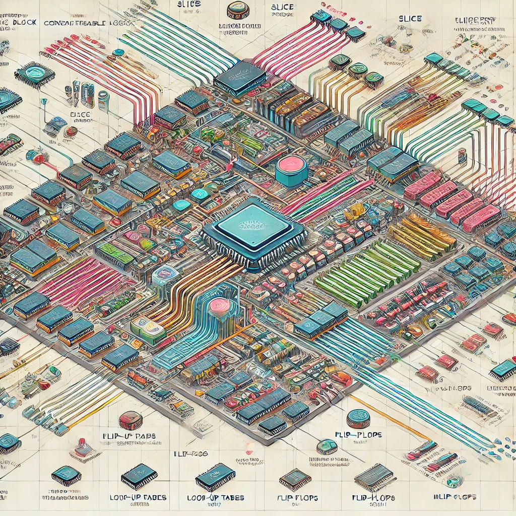
A SLICE is a smaller unit within a CLB. Each CLB typically contains multiple SLICEs, and each SLICE provides the hardware for implementing a combination of logic functions, including:
SLICEs offer flexibility in logic design, allowing designers to combine multiple smaller operations within one FPGA.
| Component | SLICE | CLB |
|---|---|---|
| Size | Smallest logic unit within a CLB | A collection of multiple SLICEs |
| Resources | Contains LUTs, flip-flops, and multiplexers | Contains several SLICEs and additional routing and I/O resources |
| Function | Executes individual logic functions | Provides a larger, more complex logical block with integrated SLICEs |
SLICEs are crucial because they allow designers to partition complex designs into smaller, more manageable blocks. By distributing the logic functions across multiple SLICEs, FPGAs achieve high parallelism, flexibility, and resource utilization.
A typical SLICE consists of:
These elements work together to handle both combinational and sequential logic, making SLICEs adaptable for a wide range of tasks.
| Component | Description |
|---|---|
| LUT (Look-Up Table) | A programmable logic array used to implement combinational logic. |
| Flip-Flops | Memory elements used to store data, enabling sequential behavior. |
| Multiplexers | Selects data sources, allowing flexible routing of signals between components. |
LUTs are the core elements of combinational logic in FPGAs. A 4-input LUT can perform any logical function with up to four inputs. When configured, the LUT stores the truth table of the logic function, allowing fast and efficient computation based on input values.
LUTs provide configurability:
By reprogramming LUTs, FPGAs can quickly adapt to new logic requirements. This flexibility makes FPGAs ideal for applications that require dynamic logic changes or custom hardware acceleration.
A Multiplexer (MUX) is a device that selects one input from several and forwards it to the output. In the context of SLICEs, multiplexers enable the routing of signals through various paths, which can be dynamically controlled based on the configuration.
Multiplexers are used to route signals within the SLICE, providing the FPGA with the ability to perform complex operations like:
Multiplexers help minimize the need for excessive wiring in the FPGA and improve the routing density. This reduces signal congestion and helps optimize the overall design.
Flip-flops are critical for implementing sequential logic. They store values and pass them along through successive clock cycles, enabling state-dependent operations. They are essential for creating systems that depend on previous inputs or states.
Each flip-flop in a SLICE holds one bit of data, which can be updated on every clock cycle. Flip-flops work together with LUTs to implement complex control logic and finite state machines (FSMs).
SLICEs leverage flip-flops to manage timing, ensuring that logic operates in sync with the clock signal. This enables the implementation of timing-sensitive operations such as counters, registers, and FSMs.
Routing is the process of directing signals between different logic blocks in the FPGA. Efficient routing is key to optimizing an FPGA design, as it directly affects performance and resource utilization.
SLICEs contain internal routing resources, such as multiplexers and routing wires, to connect LUTs, flip-flops, and other logic elements. The configuration of these resources allows for efficient signal routing within the SLICE.
Efficient routing reduces signal delay and optimizes the use of resources. Minimizing the length of signal paths and using multiplexers effectively helps achieve higher performance and lower power consumption.
| Feature | Xilinx FPGAs | Intel/Altera FPGAs |
|---|---|---|
| LUT Structure | Typically 6-input LUTs | Various configurations, often smaller LUTs |
| Flip-Flops | Up to 2 flip-flops per SLICE | Varies, sometimes fewer flip-flops |
| Additional Resources | Dedicated DSPs and block RAM | Custom logic elements, including memory blocks |
Efficient use of SLICEs in FPGA designs is crucial for achieving optimal performance, resource utilization, and minimizing power consumption. Inefficiencies in SLICE usage can lead to:
Optimizing SLICE utilization ensures that the design runs faster, consumes less power, and occupies less physical space on the FPGA.
Several strategies can be employed to optimize the usage of SLICEs in FPGA designs:
| Strategy | Description |
|---|---|
| Logic Sharing | Reuse common logic functions across multiple parts of the design to reduce the number of LUTs needed. |
| Efficient Routing | Plan the interconnections carefully to reduce the routing overhead and minimize delay. |
| Pipelining | Break down complex tasks into smaller stages to allow faster clock speeds and reduce the load on individual SLICEs. |
| Resource Sharing | Combine similar operations into the same SLICE, such as using the same flip-flop for different operations at different times. |
Each of these strategies contributes to maximizing the density and performance of the FPGA design while using fewer resources.
Here are some best practices for working with SLICEs:
By following these guidelines, designers can ensure that SLICEs are used efficiently, balancing performance, power, and resource utilization.
One common mistake is the overuse of LUTs in situations where simpler logic could suffice. This can lead to unnecessary resource consumption and increased power usage. To avoid this, ensure that complex logic functions are necessary before using large LUTs, and consider alternative implementations (e.g., using DSP blocks or hard logic).
Inefficient routing can create long signal paths, leading to increased delay and higher power consumption. To avoid this, always check that the signal routing is as short and direct as possible. Use FPGA design tools to automate routing or to visualize potential bottlenecks in the design.
Modern FPGA development environments (like Vivado for Xilinx or Quartus for Intel FPGAs) are powerful tools that provide detailed optimization reports. Ignoring these tools or not fully utilizing their capabilities can lead to suboptimal SLICE utilization and overall design performance.
While flip-flops are crucial for sequential logic, excessive use of flip-flops can waste resources. In many cases, especially in combinational logic, other design elements can be used to handle state transitions or temporary storage more efficiently.
Power efficiency is often overlooked, especially when optimizing for speed or logic density. Inefficient SLICE configurations can lead to excessive power draw. Incorporating low-power techniques like reducing clock speeds or minimizing the number of active components can extend the lifespan of the FPGA and reduce cooling requirements.
DSP blocks are specialized hardware elements integrated into many modern FPGAs for high-performance signal processing tasks (like filtering, multiplication, and FFTs). Combining SLICEs with DSP blocks can significantly reduce the logic load on individual SLICEs, improving performance and efficiency in signal-heavy applications.
Many FPGAs feature embedded memory blocks within their CLBs or near their SLICEs. These blocks can reduce the need for flip-flops by providing high-speed memory storage close to the logic, speeding up read/write operations and minimizing latency.
Some FPGAs allow for custom logic blocks that integrate directly into the SLICE, improving flexibility and performance. By designing custom arithmetic logic units (ALUs) or integrating custom state machines, you can take full advantage of FPGA resources and optimize for specific tasks.
In high-speed communication systems, SLICEs are used to implement complex modulation and demodulation algorithms, error correction, and packet processing. By using LUTs and flip-flops efficiently, designers can implement robust, real-time processing within tight power and area constraints.
In image and video processing, SLICEs are used to handle operations like convolution for filtering, transform coding (e.g., FFTs), and motion detection. By leveraging DSP blocks alongside SLICEs, FPGAs can perform these operations in parallel, achieving high throughput at lower latency compared to CPU-based implementations.
SLICEs are also used in the acceleration of machine learning inference tasks. For example, implementing neural networks or decision trees can be done more efficiently on FPGA hardware compared to software-based methods. FPGAs provide the flexibility to design custom logic tailored to the specific algorithm.
Future FPGAs are likely to feature AI-optimized SLICEs, integrated with specialized blocks for tasks like neural network inference and deep learning acceleration. This will provide even higher performance for AI applications, where both parallel processing and flexible logic are required.
As FPGAs are built with smaller and more advanced technology nodes, the density of SLICEs will increase, allowing for more complex designs in a smaller space. This will continue to enhance the capabilities of FPGAs for more demanding applications in areas like high-frequency trading, 5G, and advanced robotics.
In the future, we may see further integration of SLICEs with other types of programmable logic, such as CPU cores, GPU cores, or neural network processors. This heterogeneous computing will allow FPGAs to execute even more diverse workloads, creating new possibilities in embedded systems and high-performance computing.
SLICEs play a pivotal role in FPGA architecture, providing the basic building blocks for custom digital logic implementations. By understanding their internal structure, optimizing their usage, and avoiding common mistakes, designers can harness the full potential of FPGAs for a wide variety of applications. As FPGA technology continues to evolve, SLICEs will remain at the heart of the design process, enabling cutting-edge performance in communications, signal processing, machine learning, and beyond.
A SLICE is the basic unit of a Configurable Logic Block (CLB) in an FPGA, containing resources like LUTs, flip-flops, and multiplexers to implement logic functions.
Different FPGA manufacturers, such as Xilinx and Intel/Altera, have varying SLICE architectures. Xilinx typically uses 6-input LUTs, while Intel might use smaller LUTs for specific applications. Each has strengths depending on the design goals.
Yes, SLICEs can implement sequential logic using flip-flops to store state information and LUTs to process logic functions. This is essential for building finite state machines (FSMs) or counters.
Key strategies include logic sharing, efficient routing, and pipelining to minimize resource usage while maintaining performance.
DSP blocks handle intensive tasks like multiplication or filtering, freeing up SLICE resources for other tasks. Together, they allow for optimized performance in signal processing and data-heavy applications.
The future of SLICEs in FPGA design includes tighter integration with AI accelerators, increased logic density with smaller process nodes, and support for heterogeneous computing, combining CPU, GPU, and custom logic in one device.
