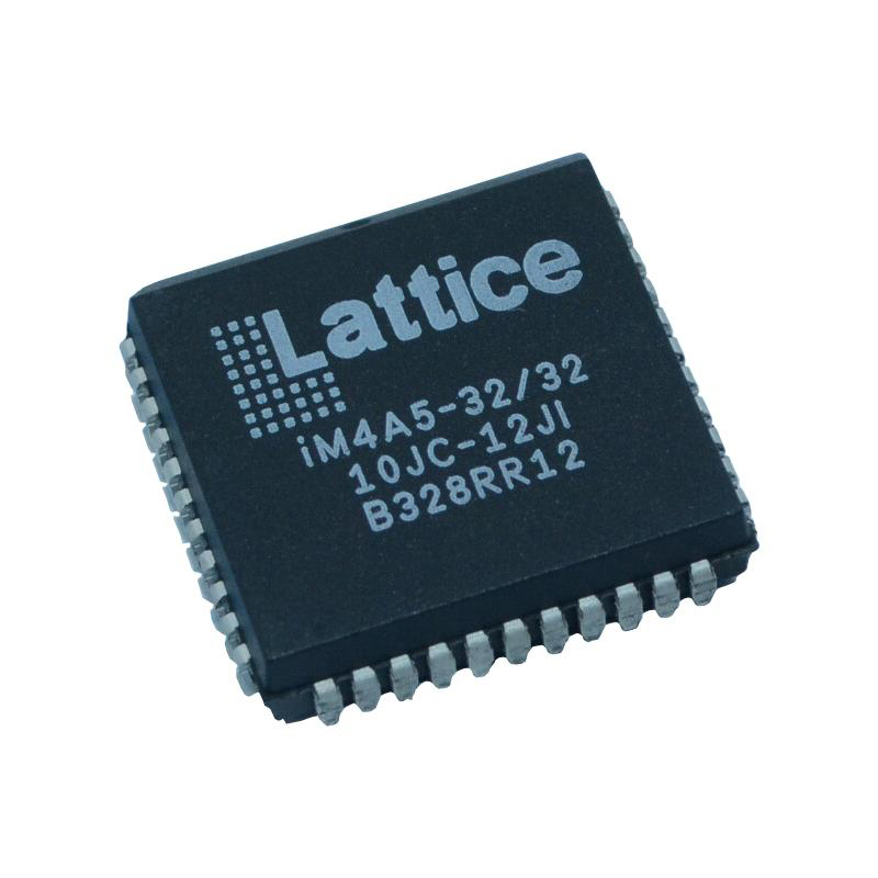
A variety of high bandwidth sensor and display interfaces, video processing, and machine learning inferencing are supported by the CrossLink-NX line of low-power FPGAs, which are ideal for bridging and processing demands in embedded vision applications. It is constructed utilizing low-power 28 nm FD-SOI technology on the Lattice Nexus FPGA platform. It offers tiny footprint packaging alternatives and combines the extraordinary flexibility of an FPGA with the low power and high reliability (because to an exceptionally low SER) of FD-SOI technology.
Numerous interfaces are supported by CrossLink-NX, including SGMII (Gigabit Ethernet), LVDS, SLVS, subLVDS, PCI Express (Gen1, Gen2), and MIPI D-PHY (CSI-2, DSI). Up to 39K logic cells, 56 18x18 multipliers, 2.9 Mb of embedded memory made up of EBR and LRAM blocks, distributed memory, DRAM interfaces (supporting DDR3, DDR3L, LPDDR2, LPDDR3 up to 1066 Mbps x 16 data width), and ALU building blocks for soft processors are just a few of the processing features of CrossLink-NX. The reconfigurable SRAM-based logic fabric, ultra-fast configuration of the programmable sysI/O, and TransFR field upgrading feature are all supported by CrossLink-NX FPGAs. Password protection and bitstream encryption are security features for user designs. The extremely low SER of FD-SOI technology lends itself to good reliability, but it also supports active reliability measures like built-in frame-based SED/SEC (for SRAM-based logic fabric) and ECC (for EBR and LRAM). Each device has an integrated ADC that can be used for system monitoring purposes. Large sophisticated user designs can be efficiently realized on the CrossLink-NX FPGA series thanks to Lattice Radiant design software.
Popular logic synthesis programs offer support for synthesis libraries for CrossLink-NX devices. Radiant Tools places and routes the user design in the CrossLinkNX device using the output from the synthesis tool and limitations from its floor planning tools. In order to verify timing, the tools extract timing from the routing and back-annotate it into the design. For the CrossLink-NX family, Lattice offers a variety of pre-engineered IP (Intellectual Property) modules. Utilizing these standardized blocks of configurable soft IP cores allows you to focus on the distinctive features of your design, boosting productivity.
Features
Programmable Architecture
17K to 39K logic cells
24 to 56 18 x 18 multipliers (in sysDSPblocks)
2.5 to 2.9 Mb of embedded memory blocks(EBR, LRAM)
36 to 192 programmable sysI/O (HighPerformance and Wide Range I/O)
MIPI D-PHY
Up to two hardened 4-lane MIPI D-PHYinterfaces
Up to 8 lanes total
Transmit or receive
Supports CSI-2, DSI
20 Gbps aggregate bandwidth
2.5Gbps per lane, 10 Gbps per D-PHYinterface
Additional Soft D-PHY interfaces supported byHigh Performance (HP) sysI/O
Transmit or receive
Supports CSI-2, DSI
Up to 1.5 Gbps per lane
Programmable sysI/O supports wide variety ofinterfaces
High Performance (HP) on bottom I/O dualrank
Supports up to 1.8 V VCCIO
Mixed voltage support (1.0 V, 1.2 V, 1.5 V,1.8 V)
High-speed differential up to 1.5 Gbps
Supports soft D-PHY (Tx/Rx), LVDS 7:1(Tx/Rx), SLVS (Tx/Rx), subLVDS (Rx)
Supports SGMII (Gb Ethernet) – 2channels (Tx/Rx) at 1.25 Gbps
Dedicated DDR3/DDR3L andLPDDR2/LPDDR3 memory support withDQS logic, up to 1066 Mbps data- rate and x16 data-width
Wide Range (WR) on Left, Right and Top I/OBanks
Supports up to 3.3 V VCCIO
Mixed voltage support (1.2 V, 1.5 V, 1.8 V,2.5 V, 3.3 V)
Programmable slew rate (slow, med, fast)
Controlled impedance mode
Emulated LVDS support
Hot-socketing
