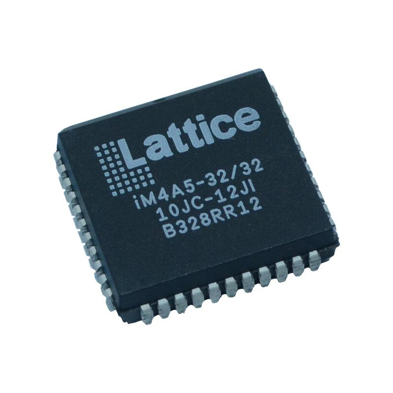
Five devices of the iCE40 LP/HX family of ultra-low power, non-volatile FPGAs have LUT densities ranging from 384 to 7,680. These devices include Embedded Block RAM (EBR), Non-volatile Configuration Memory (NVCM), and Phase Locked Loops (PLLs), in addition to LUT-based, low-cost programmable circuitry. The devices can be employed in low-cost, high-volume consumer and system applications thanks to these capabilities. High-Current drivers are available in some packages and are the best choice for driving three white LEDs or one RGB LED. The 40 nm CMOS low power technique is used to create the iCE40 LP/HX devices. Numerous aspects of the device architecture include programmable low-swing differential I/Os and the capacity to dynamically disable on-chip PLLs. All family members will experience low static power as a result of these features' assistance in controlling static and dynamic power usage. Ultra low power (LP) and high performance (HX) variants of the iCE40 LP/HX devices are both offered. The innovative halogen-free packages for the iCE40 LP/HX FPGAs range widely, from the compact 1.40 mm x 1.48 mm WLCSP to the PCB-friendly 20 mm x 20 mm TQFP. Additionally, the iCE40 LP/HX devices offer on-chip NVCM for flexible, dependable, and secure configuration. These devices can be configured by an external master, such as a CPU, or they can configure themselves via external SPI Flash. In order to effectively construct complicated designs using the iCE40 LP/HX family of devices, Lattice offers a variety of design tools. Support for the iCE40 LP/HX synthesis library is offered by well-known logic synthesis tools. Lattice design tools place and route the design in the iCE40 LP/HX device using the output from the synthesis tool as well as the user's preferences and constraints. In order to verify timing, these tools extract timing from the routing and back-annotate it into the design. Many pre-engineered IP (Intellectual Property) modules are available from Lattice, including a variety of reference designs that are free to use and are licensed for the iCE40 LP/HX FPGA family. Users are liberated to focus on the distinctive features of their designs, boosting productivity, by employing these adjustable soft core IP cores as standardized building blocks.
Features
Flexible Logic Architecture
Five devices with 384 to 7,680 LUT4s and 10 to 206 I/Os
Ultra-low Power Devices
Advanced 40 nm low power process
As low as 21 µA standby power
Programmable low swing differential I/Os
Embedded and Distributed Memory
Up to 128 kb sysMEM Embedded Block RAM
Pre-Engineered Source Synchronous I/O
DDR registers in I/O cells
High Current LED Drivers
Three High Current Drivers used for three different LEDs or one RGB LED
High Performance, Flexible I/O Buffer
Programmable sysI/O buffer supports wide range of interfaces:
LVCMOS 3.3/2.5/1.8
LVDS25E, subLVDS
Schmitt trigger inputs, to 200 mV typical hysteresis
Programmable pull-up mode
Flexible On-Chip Clocking
Eight low skew global signal resources
Up to two analog PLLs per device
Flexible Device Configuration
SRAM is configured through:
Standard SPI Interface
Internal Nonvolatile Configuration Memory (NVCM)
Broad Range of Package Options
WLCSP, QFN, VQFP, TQFP, ucBGA, caBGA, and csBGA package options
Small footprint package options
As small as 1.40 mm x 1.48 mm
Advanced halogen-free packaging
