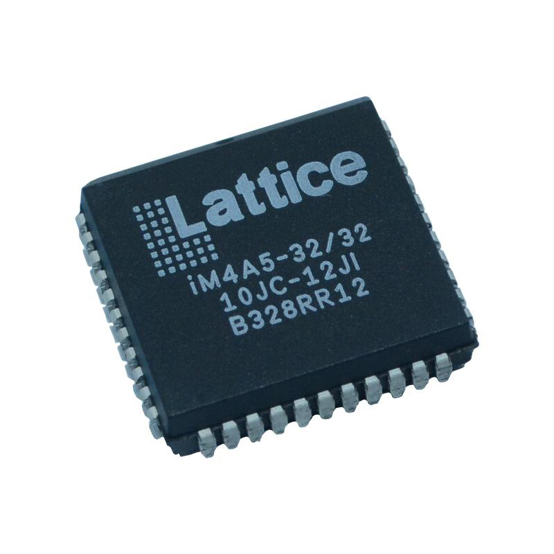
Description
For the lowest static and dynamic power consumption of any similar CPLD or FPGA device, the Lattice Semiconductor iCE65 programmable logic family was created. The on-chip, nonvolatile configuration memory (NVCM) on iCE65 devices allows for customization for a particular application and is suited for cost-sensitive, high-volume applications. The configuration image saved in an external commodity SPI serial Flash PROM can be used by iCE65 devices to self-configure them, or it can be downloaded from an external CPU over an SPI-like serial port.
Each iCE65 device consists of four primary architectural elements.
An array of Programmable Logic Blocks (PLBs)
Each PLB contains eight Logic Cells (LCs); each Logic Cell consists of …
A fast, four-input look-up table (LUT4) capable of implementing any combinational logic function of up to four inputs, regardless of complexity
A ‘D’-type flip-flop with an optional clock-enable and set/reset control
Fast carry logic to accelerate arithmetic functions such as adders, subtracters, comparators, and counters.
Common clock input with polarity control, clock-enable input, and optional set/reset control input to
the PLB is shared among all eight Logic Cells
Two-port, 4Kbit RAM blocks (RAM4K)
256x16 default configuration; selectable data width using programmable logic resources
Simultaneous read and write access; ideal for FIFO memory and data buffering applications
RAM contents pre-loadable during configuration
Four I/O banks with independent supply voltage, each with multiple Programmable Input/Output (PIO)
blocks
LVCMOS I/O standards and LVDS outputs supported in all banks
I/O Bank 3 supports additional SSTL, MDDR, LVDS, and SubLVDS I/O standards
Programmable interconnections between the blocks
Flexible connections between all programmable logic functions
Eight dedicated low-skew, high-fanout clock distribution networks
