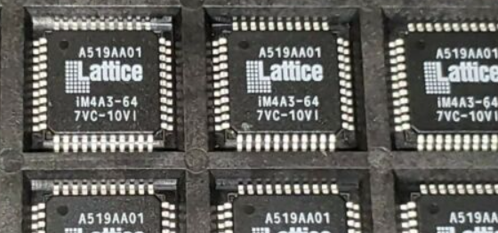
The Lattice ispMACH 4A series, with its extraordinarily flexible architecture, offers a superior Complex Programmable Logic Device (CPLD) combination of user-friendly silicon components and software tools. Users will often gain from a CPLD solution that is dependable and predictable, as well as from faster time to market, greater flexibility, and lower costs. The ispMACH 4A devices offer macrocell densities of 32 to 512 with pin-out retention of 100%. Operation is supported at 3.3-V (M4A3-xxx) and 5-V by the ispMACH 4A families (M4A5-xxx). It is possible to in-system program ispMACH 4A devices at 5-V or 3.3-V via the JTAG (IEEE Std. 1149.1) interface. JTAG boundary scan testing also enables product testability on automated test equipment for device connectivity. Every member of the ispMACH 4A family enables First-Time-Fit and straightforward system integration with pin-out retention after any design modification and refit. The ispMACH 4A products may provide reliable fixed timing for 3.3-V and 5-V operation as soon as 5.0 ns tPD and 182 MHz fCNT thanks to the SpeedLocking function and up to 20 product terms per output.
FUNCTIONAL DESCRIPTION
The center switch matrix facilitates communication between the PAL blocks and directs inputs to the PAL blocks. The logic designer may create sophisticated designs with just the core switch matrix and PAL blocks, as opposed to using many devices. To use these gadgets successfully, link networks are necessary. The ispMACH 4A design offers variable coupling of the macrocells to the product terms and the I/O pins to the macrocells through the use of the output switch matrix and logic allocator. More input routing options are provided via the input switch matrix. These materials provide the flexibility needed to effectively fit designs.
FEATURES
◆ High-performance, E2 CMOS 3.3-V & 5-V CPLD families
◆ Flexible architecture for rapid logic designs
— Excellent First-Time-FitTM and refit feature
— SpeedLockingTM performance for guaranteed fixed timing
— Central, input and output switch matrices for 100% routability and 100% pin-out retention
◆ High speed
— 5.0ns tPD Commercial and 7.5ns tPD Industrial
— 182MHz fCNT
◆ 32 to 512 macrocells; 32 to 768 registers
◆ 44 to 388 pins in PLCC, PQFP, TQFP, BGA, fpBGA and caBGA packages
◆ Flexible architecture for a wide range of design styles
— D/T registers and latches
— Synchronous or asynchronous mode
— Dedicated input registers
— Programmable polarity
— Reset/ preset swapping
◆ Advanced capabilities for easy system integration
— 3.3-V & 5-V JEDEC-compliant operations
— JTAG (IEEE 1149.1) compliant for boundary scan testing
— 3.3-V & 5-V JTAG in-system programming
— PCI compliant (-5/-55/-6/-65/-7/-10/-12 speed grades)
— Safe for mixed supply voltage system designs
— Programmable pull-up or Bus-FriendlyTM inputs and I/Os
— Hot-socketing
— Programmable security bit
— Individual output slew rate control
◆ Advanced E2 CMOS process provides high-performance, cost-effective solutions
◆ Lead-free package options
