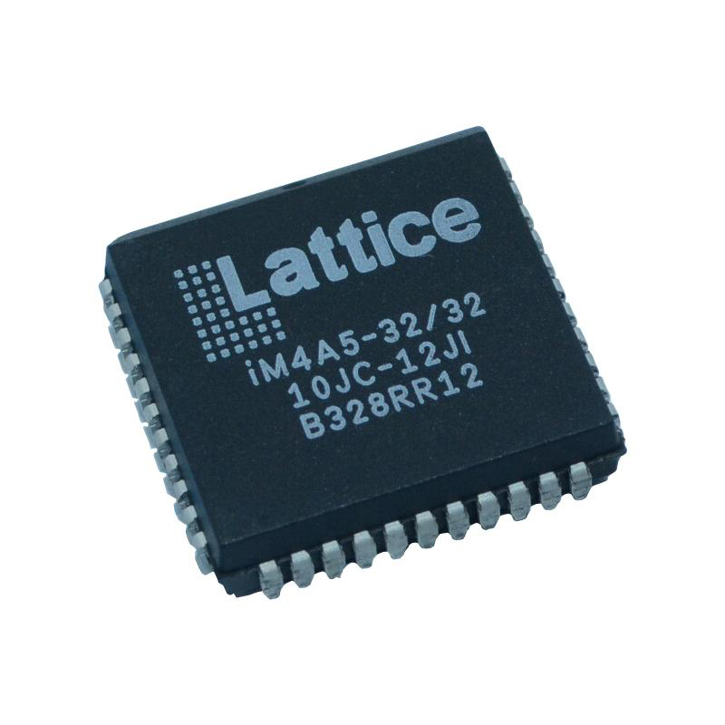
The ispXPGA family of devices offers the perfect platform for the development of high-performance, non-volatile, indefinitely reprogrammable logic architectures. Other FPGA options, which are either re-programmable or non-volatile, demand a trade-off. This family combines this capacity with a common architecture that has the features necessary for system-level design in the modern era.
Two alternatives are offered for the ispXPGA family. While the less expensive "E-Series" supports the same high-performance FPGA fabric without the sys- HSI Block, the standard device supports sysHSI capabilities for extremely rapid serial connections.
The non-volatile functionality of the ispXPGA family is provided by Electrically Erasable CMOS (E2CMOS) memory cells. These make it possible for logic to start working a few microseconds after power is introduced, making interfacing in many applications simple. With this functionality, designs can be protected from unwanted readback and expensive external configuration memories are not necessary. The device may, if desired, be infinitely reconfigured thanks to internal SRAM cells. The IEEE 1532 industry standard allows for the programming and verification of SRAM and E2CMOS cells alike. The sysCONFIGIM peripheral port also allows for the configuration and readback of the SRAM cells.The family covers the 139K to 1.25M functional gate density and 160 to 496 /0 range needed for the majority of today's logic circuits. The devices can operate on 1.8V, 2.5V, and 3.3V power supply, allowing for simple system integration.
The integration of sysMEM dual-port memory blocks, sysIO enhanced /O support, and sysCLOCK Phase Locked Loops (PLLs) meets system-level design requirements. Numerous sysHSI blocks, which offer serialization/de-serialization (SERDES) and clock data recovery (CDR), facilitate high-speed serial communications.
The Lattice company's ispl EVERTM design tool enables simple execution of designs utilizing its ispXPGA product. Major logic synthesis tools have support for synthesis libraries. The design is placed and routed in the ispXPGA product using the output from these popular synthesis tools provided by the ispL EVER tool. The tool aids in floor layout and the control of other device limits. The tool also generates results for widely used timing analysis tools, such as:
For the ispXPGA device, Lattice offers a selection of pre-designed modules known as IP cores to boost designer productivity. These JIP cores enable designers to focus on the distinctive aspects of their designs while implementing common functionalities like memory controllers, bus interfaces, and common communication interfaces using pre-designed blocks.
Thanks to the use of cutting-edge technology and innovative architecture, the ispXPGA FPGA devices provide designers outstanding speed performance. Although it varies on the design, several typical systems can operate at speeds more than 150MHz. Some designs are capable of reaching at least 300MHz.
Functional
Programmable Function Unit
The ispXPGA architecture's fundamental building piece is the Programmable Function Unit (PFU). The PFUs are organized in the device in rows and columns, with PFU (1,1) designating (row1, column 1). Each PFU has a Wide Logic Generator (WLG), four Configurable Logic Elements (CLEs), and four Configurable Sequential Elements (CSEs). These elements can be used by the PFU to implement a number of functions.
Each PFU has nine outputs and 57 inputs. Twenty inputs are used by the PFU for logic, and 37 inputs are used to drive the control logic, which generates six control signals for the PFU.
