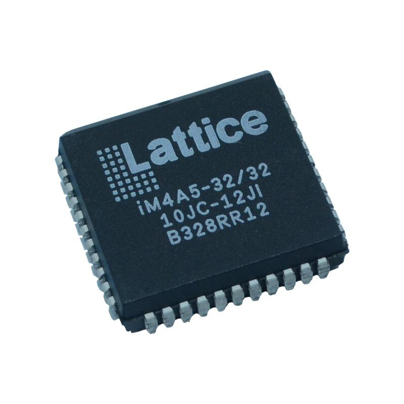
Description
By enabling flexible memory and the flexibility to balance memory and logic resources within the device, these devices enhance the functionality of Lattice's well-known SuperWIDE CPLD design. The family is compatible with ternary CAM, FIFO, true dual-port SRAM, single-port SRAM, and true dual-port SRAM. SysIO interfaces and sysCLOCK PLLs also offer assistance to improve system performance.The gadgets offer designers a practical one-chip solution that offers design security, extraordinary reconfigurability, and logic availability at bootup. Utilizing cutting-edge process technology results in performance that leads the industry, with combinatorial propagation delay as low as 4.0ns, clock-to-out latency as low as 2.8ns, setup time as low as 2.5ns, and operating frequency as high as 285MHz. Along with this performance, power consumption is both static and dynamically low. Predictable deterministic timing is provided by the ispXPLD 5000MX architecture. Users may overcome the issue of today's mixed voltage designs thanks to the availability of 3.3, 2.5, and 1.8V variants of these devices (designated the 5000MV, 5000MB, and 5000MC series, respectively), as well as the flexibility of the sysIO interface. The testability of boundary scans facilitates incorporation into the sophisticated systems of today. The likelihood of a successful fit for a specific application is increased by a range of density and package alternatives. To guarantee that various density devices in the same package have compatible pin-outs, the ispXPLD 5000MX family was created. When undertaking design migration from lower density components to higher density parts, the architecture further guarantees a high success rate.
Functional
The ispXPLD devices may address common system functions that were previously restricted to FPGAs or ASICs because of the combination of system-level functionality, memory, and logic. Great application flexibility is provided by the integration of many independent blocks of buffer memory employing a variety of memory architectures (FIFO, dual-port, CAM, etc.) along with quick programmable logic into a single device. The usefulness of the devices as effective control and data conductors within cutting-edge systems is increased by the addition of programmable sysIO interface standard support and sysCLOCK high-performance clocking. High-performance bus bridges, intelligent backplane interfaces, protocol processors, and similar devices are examples of potential application areas. The architecture takes advantage of the characteristics of conventional CPLDs and targets high-density, high-performance (up to 285 MHz) applications for sectors that demand quick time to market. These sectors include data processing, data communications, and telecommunications. Switches, exchange equipment, and cellular base stations are examples of common telecommunications applications. High-end routers, bridges, switches, repeaters, and intelligent hubs are examples of common applications in data communications. Disk-array systems, data storage, RAID controllers, high-end graphics, high-end servers, scanners, and imaging systems are examples of common applications in data processing.
Feature
The two largest segments of the high density programmable logic market have traditionally been nonvolatile, Complex Programmable Logic Devices (CPLDs) and SRAM-based Field Programmable Gate Arrays (FPGAs). CPLDs have historically provided the benefits of
ƒ Fast, predictable timing
ƒ Single-level wide logic support
ƒ Non-volatile, in-system programmability (ISP)
ƒ "Instant on" operation while SRAM-based FPGAs have provided
ƒ Very high logic density
ƒ On-chip Memory Support
ƒ Unlimited in-system reconfigurability
ƒ Low standby power
Lattice Semiconductor has developed a logical successor to earlier Simple PLD and Complex PLD architectures, called the ispXPLD (eXpanded Programmable Logic Device), that combines the best attributes of CPLDs and FPGAs in a single architecture. These new devices are based upon a convergence of programming technology and architecture that is truly unique. The new programming technology, called ispXP (for in-system programmable eXpanded Programmability), provides non-volatile in-system programmability combined with reconfigurability via a microprocessor sysCONFIG port. The new architecture, based on a set of homogeneous Multi-FunctionBlocks that can implement a variety of functions based on the user's application requirements, supports both logic and memory on-chip with up to 300K system gates in a single device. In addition, extremely wide functions of up to 136 inputs can be implemented in a single level of logic for wide parallel logic processing.
