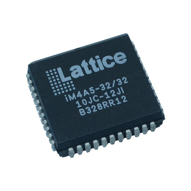
In a single, market-leading architecture, the LatticeSC series of FPGAs includes a high-performance FPGA fabric, high-performance I/Os, and substantial embedded RAM. Additionally, every LatticeSC device includes up to 32 embedded SERDES channels with corresponding Physical Coding Sublayer (PCS) circuitry. Numerous high-speed data transfer protocols that are industry standards can be supported by the flexiPCS logic. FlexiPCS circuitry has separate transmit and receive SERDES on each channel enabling full-duplex, high-speed serial data transfers up to 3.8 Gbps. For example, SONET (STS-12/STS-12c, STS-48/STS-48c, and TFI-5 support of 10 Gbps or above), Gigabit Ethernet (compliant with the IEEE 1000BASE-X specification), 1.02 or 2.04 Gbps Fibre Channel, PCI Express, and Serial RapidIO can all be supported by the PCS logic in each channel. Additionally, a variety of configurations allow for the entire or partial bypass of the protocol-based logic, giving users more freedom to create their own high-speed data interfaces. It is possible to support protocols that demand data rates higher than 3.8 Gbps by designating either one pair or all four channels in a PCS quad block to one data connection. Full-duplex serial data transfers at up to 15.2 Gbps can be supported by a single quad. A single PCS quad can be set up to provide x4 PCI Express, 4x RapidIO, 10Gb Ethernet (with a fully compliant XAUI interface), and 10Gb Fibre Channel. Additionally, the PCS has bypass modes that enable an 8-bit or 10-bit direct communication from the SERDES to the FPGA logic. For applications like Serial Digital Video, each SERDES pin can also be individually DC coupled, enabling high-speed and low-speed operation on the single SERDES pin.
