Time: 2025-03-12 11:28:26View:
Implementing Gigabit Ethernet on an Altera FPGA (now part of Intel FPGA) involves leveraging the FPGA's programmable logic and hard IP blocks to handle high-speed data transmission and network protocols. Below is a detailed solution for implementing Gigabit Ethernet on an Altera FPGA:
System Overview
The implementation involves the following key components:
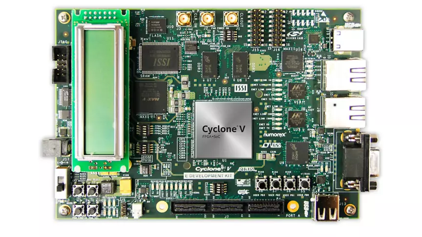
1. FPGA: Altera/Intel FPGA with integrated Gigabit Ethernet hard IP (e.g., Cyclone V, Arria 10).
2. PHY Chip: External Ethernet PHY chip (e.g., Marvell 88E1111) to handle physical layer signaling.
3. MAC Layer: Implemented in FPGA logic or using hard IP blocks.
4. Protocol Stack: Lightweight TCP/IP stack or custom protocol handling.
5. Memory: On-chip or external memory for buffering and packet processing.
1. FPGA Selection:
Choose an FPGA with integrated Gigabit Ethernet hard IP blocks (e.g., Intel Cyclone V, Arria 10).
Ensure the FPGA has sufficient logic elements, memory, and I/O pins for your application.
2.Ethernet PHY:
Use an external Gigabit Ethernet PHY chip (e.g., Marvell 88E1111, Realtek RTL8211).
Connect the PHY to the FPGA via RGMII (Reduced Gigabit Media Independent Interface) or GMII (Gigabit Media Independent Interface).
3. Clock and Reset:
Provide a 125 MHz reference clock for RGMII or 25 MHz for GMII.
Ensure proper reset sequencing for the PHY and FPGA.
4. Interfaces:
RGMII/GMII: Connects the FPGA to the PHY chip.
MDIO/MDC: For PHY configuration and status monitoring.
SGMII: If using a serial interface for longer-distance connections.
1. MAC Layer:
Use the FPGA's hard IP blocks for the Ethernet MAC layer if available.
Alternatively, implement a soft MAC core in HDL (e.g., Verilog/VHDL).
2. Packet Processing:
Implement packet buffering using on-chip RAM or external DDR memory.
Use FIFOs for data flow control between the MAC and upper layers.
3. Protocol Stack:
Implement a lightweight TCP/IP stack in the FPGA or use a soft-core processor (e.g., Nios II) to handle higher-layer protocols.
For custom applications, implement only the required protocols (e.g., UDP, ARP, ICMP).
4. DMA Engine:
Implement a DMA engine for efficient data transfer between the Ethernet MAC and memory.
1. PHY Configuration:
Use the MDIO interface to configure the PHY chip (e.g., set speed, duplex mode, auto-negotiation).
2. Protocol Handling:
If using a soft-core processor (e.g., Nios II), implement the TCP/IP stack in software.
For custom applications, implement protocol handling in hardware (e.g., UDP packet parsing).
3. Application Logic:
Implement the application-specific logic (e.g., data processing, control logic).
1. Intel Quartus Prime:
Use Quartus Prime for FPGA design, synthesis, and simulation.
Leverage the Platform Designer (formerly Qsys) tool to integrate IP blocks.
2. Simulation:
Use ModelSim or QuestaSim for functional simulation of the Ethernet MAC and protocol stack.
3. Debugging:
Use SignalTap Logic Analyzer for real-time debugging of the FPGA design.
1. Set Up Hardware:
Connect the FPGA to the Ethernet PHY chip using RGMII/GMII.
Provide the necessary clocks and power supplies.
2. Design MAC Layer:
Configure the Ethernet MAC hard IP or implement a soft MAC core.
Integrate the MAC with the PHY interface.
3. Implement Packet Buffering:
Design FIFOs or memory buffers for packet storage.
Implement a DMA engine for efficient data transfer.
4. Develop Protocol Stack:
Implement the required protocols (e.g., UDP, ARP) in hardware or software.
Test the protocol stack using simulation and hardware testing.
5. Integrate Application Logic:
Add the application-specific logic to process and generate Ethernet packets.
Test the complete system with real-world traffic.
1. FPGA: Intel Cyclone V with integrated Gigabit Ethernet hard IP.
2. PHY Chip: Marvell 88E1111 connected via RGMII.
3. MAC Layer: Use the FPGA's hard IP for the Ethernet MAC.
4. Protocol Stack: Implement UDP/IP in hardware for low-latency communication.
5. Application: High-speed data acquisition system sending data over Ethernet.
1. Timing Closure:
Use proper timing constraints and optimize the design for high-speed operation.
Use pipelining and register retiming to meet timing requirements.
2. Resource Utilization:
Optimize the design to fit within the FPGA's resources.
Use compression techniques for packet headers if necessary.
3. Interoperability:
Test the design with different Ethernet devices to ensure compatibility.
Follow IEEE 802.3 standards for Ethernet implementation.
By following this approach, you can successfully implement Gigabit Ethernet on an Altera FPGA, enabling high-speed network communication for your application.
