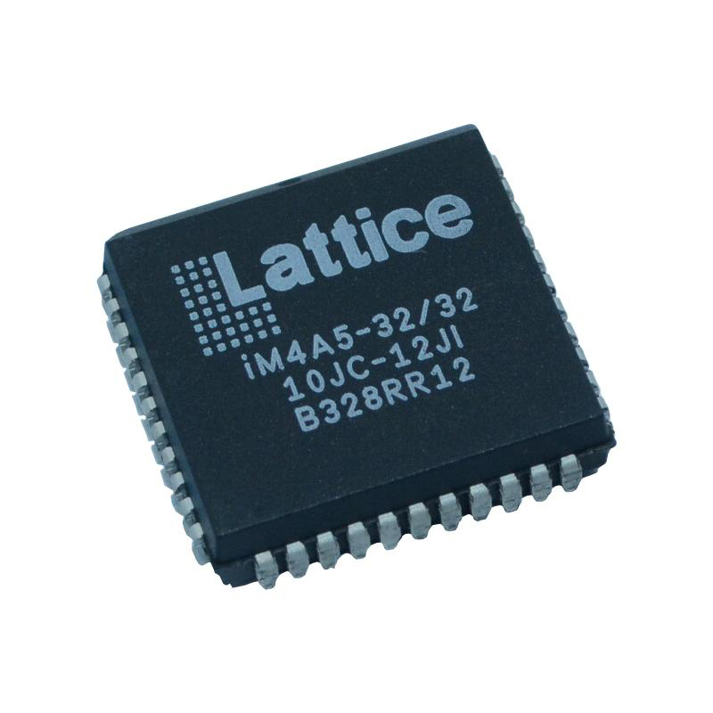
A programmable video bridging device called CrossLinkPlus from Lattice Semiconductor supports numerous protocols and interfaces for mobile image sensors and screens. The system is built using embedded flash and Lattice mobile FPGA 40-nm technology. It is a small-footprint, low-power FPGA that boots up quickly (in less than 10 ms).
CrossLinkPlus supports a variety of video interfaces, including SLVS200, subLVDS, HiSPi, OpenLDI, FPD-Link, MIPI D-PHY, MIPI CSI-2, MIPI DSI, CMOS camera and display interfaces, and more. For CrossLinkPlus, Lattice Semiconductor offers a variety of pre-engineered Intellectual Property (IP) modules.
People may focus on the distinctive features of your design while also enhancing efficiency by employing these adjustable soft core IPs as standardized building blocks. CrossLinkPlus can be used to effectively implement huge, complicated designs created with the Lattice Diamond design program. Popular logic synthesis programs offer support for synthesis libraries for CrossLinkPlus devices. The Diamond tools install and route the design in the CrossLinkPlus device using the output from the synthesis tool and the limitations from its floor planning tools. For timing verification, the tools extract the time from the routing and back-annotate it into the design. The interfaces on CrossLinkPlus offer a range of bridging options for the neighboring ISM markets as well as the smart phone, tablet, wearables, VR, AR, drone, smart home, and HMI industries. The system can accommodate content with high resolution and bandwidth for mobile cameras and displays at four UHD and higher.
Features
Ultra-low power
Sleep mode support
Normal Operation – from 5 mW to 150 mW
Ultra small footprint packages
64-ball ucfBGA (12 mm2) Programmable architecture
5936 LUTs
180 kb block RAM
47 kb distributed RAM
Two hardened 4-lane MIPI D-PHY interfaces
Transmit and receive
6 Gb/s per D-PHY interface
Programmable source synchronous I/O
MIPI D-PHY Rx, LVDS Rx, LVDS Tx, subLVDS Rx, SLVS200 Rx, HiSPi Rx
Up to 1200 Mb/s per I/O
Four high-speed clock inputs
Programmable CMOS I/O
LVTTL and LVCMOS
3.3 V, 2.5 V, 1.8 V and 1.2 V (outputs)
LVCMOS differential outputs
Flexible device configuration
On-chip reconfigurable Flash
Master SPI boot from external flash
Dual image booting supported
I2C programming
SPI programming
TransFR I/O for simple field updates
Enhanced system level support
Reveal logic analyzer
TraceID for system tracking
On-chip hardened I2C block
Applications examples
Dual MIPI CSI-2 to Single MIPI CSI-2 Aggregation
Quad MIPI CSI-2 to Single MIPI CSI-2 Aggregation
Single MIPI DSI to Single MIPI DSI Repeater
Single MIPI CSI-2 to Single MIPI CSI-2 Repeater
Single MIPI DSI to Dual MIPI DSI Splitter
Single MIPI CSI-2 to Dual MIPI CSI-2 Splitter
MIPI DSI to OpenLDI/FPD-Link/LVDS Translator
OpenLDI/FPD-Link/LVDS to MIPI DSI Translator
MIPI DSI/CSI-2 to CMOS Translator
CMOS to MIPI DSI/CSI-2 Translator
subLVDS to MIPI CSI-2 Translator
