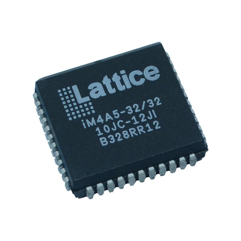
An in-system programmable zero delay global fan-out buffer for clock distribution applications is the ispClock5300S. The initial member of the ispClock5300S series, the ispClock5312S, offers up to 12 single-ended very low skew outputs. It is possible to separately configure each pair of outputs to accommodate a different output frequency and I/O standard (LVTTL, LVCMOS -3.3V, 2.5V, 1.8, SSTL, HSTL). Each output also offers independent, programmable termination, slew-rate, and timing skew control. All configuration data is kept in non-volatile E2 CMOS memory on the chip.
Using the on-chip low jitter high-performance PLL, the ispClock5300S devices offer exceptionally short propagation delay (zero-delay) from input to output. Three PLL clock-derived frequencies can be produced by a group of three programmable 5-bit counters. Only powers of 2 can be used to program these counters (1, 2, 4, 8, 16, 32). The output routing matrix can then be used to route the clock output from any of the V-dividers to any clock output pin. Additionally, the output routing matrix allows reference clock inputs to be routed straight to any output. Four different operating modes for the ispClock5300S device can be set up: zero delay buffer mode, dual non-zero delay buffer mode, non-zero delay buffer mode with output dividers, and combined zero-delay and non-zero delay buffer mode.
