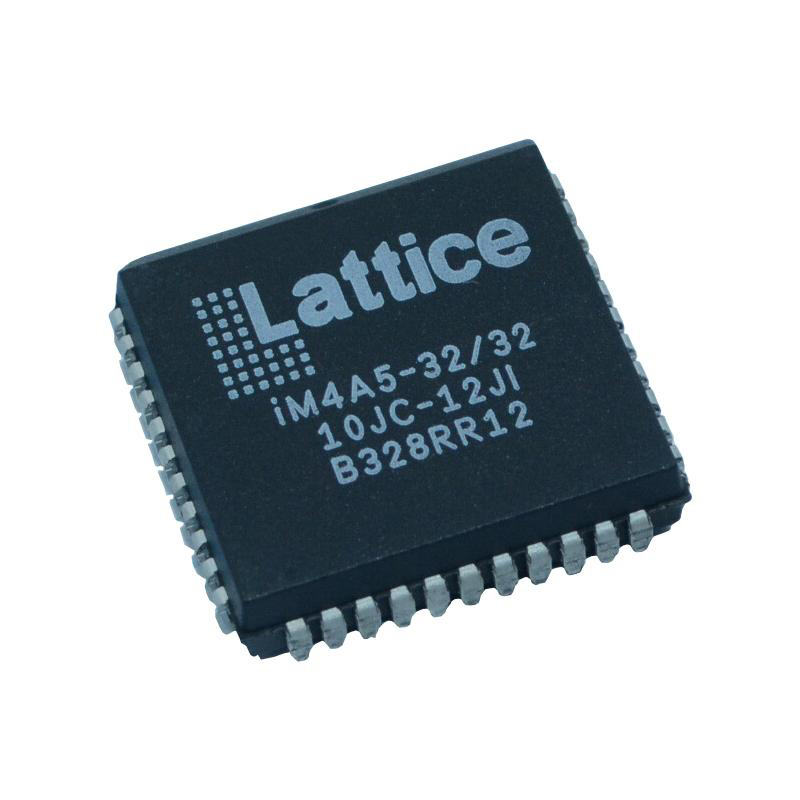
Description
It exists in every I/O cell. Each output features two multiplexer control inputs (MUX0 and MUX1), two output latch clocks (CLK, CLKEN), and separate, programmable /O tri-state control (OE) inputs. Each I/0 cell has the ability to program the polarity of these signals. Up to four signal sources can be dynamically chosen for a specific output under the direction of a quick 4:1 MUX by the MUX0 and MUX1 inputs. With the MUX expander feature of each I/O and an increase in propagation latency of 2.0ns, a larger 16:1 MUX can be built. Selected sets of I/O pins can be used to directly drive the OE, CLK, CL KEN, MUX0, and MUX1 inputs. Clock-to-output delays are kept to a minimum by optional dedicated clock input pins. The same set of I/O pins are shared by CLK and CLKEN. When CLKEN=0, the register clock is turned off. It is possible to define links between I/O pins and architectural elements (such as output enable control, registered or locked inputs or outputs, etc.) through in-system programming. The ispGDXV devices don't have any programmable logic arrays due to their data path application focus. Schmitt trigger buffers for noise immunity are present on all input pins. The device's non-volatile E?CMOS technology is used to program these connections. With non-volatile technology, the device configuration is kept even when the power is turned off.
Additionally, there are no restrictions on pin-to-pin signal routing for 1:1 or 1:n. In other words, any 1/0 pin that is specified as an output can be driven by any l/0 pin that is defined as an input. Additionally, outputs can be adjusted to HIGH or LOW logic levels using the device pins (in jumper or DIP switch mode). Device outputs can be connected in parallel for increased drive and are designed for 24mA sink and 12mA source current (at JEDEC LVTTL levels). Each /o pin on the ispGDXVA can be individually programmed for 3.3V or 2.5V output levels, as will be explained later. Each I/0 pin can have its own independently set program- mable output slew rate control to lower overall ground bouncing and switching noise. For improved testability, IEEE1149-1-compliant Boundary Scan Test circuitry is installed on AlI/0 pins. Additionally, through a unique set of private commands, the Test Access Port supports in-system programming. To endure "Iive inser-tion" system conditions, the ispGDXV 1/Os were created. During the cycles of power-up and power-down, the /O buffers are disabled. Absolute maximum rating requirements for the Vco and I/O pins must still be met when designing for "live insertion."
Features
●IN-SYSTEM PROGRAMMABLE GENERIC DIGITALCROSSPOINT FAMILY
一Advanced Architecture Addresses Programmable PCB Interconnect, Bus Interface Integration and Jumper/Switch Replacement
一“Any Input to Any Output" Routing
- , Fixed HIGH or LOW Output Option for Jumper/DIP
Switch Emulation
- Space-Saving PQFP and BGA Packaging
- Dedicated IEEE 1149.1-Compliant Boundary ScanTest .
●HIGH PERFORMANCE E2CMOS° TECHNOLOGY
一3.3V Core Power Supply
一3.5ns Input-to-Output/3.5ns Clock-to-Output Delay*
250MHz Maximum Clock Frequency*
一TTL/3.3V/2.5V Compatible Input Thresholds and
Output Levels (Individually Programmable)"
一Low-Power: 16.5mA Quiescent Icc"
一. 24mA loL Drive with Programmable Slew RateControl Option
- PCI Compatible Drive Capability*
Schmitt Trigger Inputs for Noise Immunity
Electrically Erasable and Reprogrammable
Non-Volatile E'CMOS Technology
●ispGDXV OFFERS THE FOLLOWING ADVANTAGES
一3.3V In-System Programmable Using Boundary Scan.Test Access Port (TAP)
一Change Interconnects in Seconds
●FLEXIBLE ARCHITECTURE
一Combinatorial/Latched/Registered Inputs or Outputs
一Individual /0 Tri-state Control with Polarity Control Dedicated Clock/Clock Enable Input Pins (four) O
Programmable Clocks/Clock Enables from 1/0 Pins(40)
- Single Level 4:1 Dynamic Path Selection (Tpd = 3.5ns)
Programmable Wide-MUX Cascade Feature
Supports up to 16:1 mUX
Programmable Pull-ups, Bus HoldLatch and Open
Drain on 10 Pins
一Outputs Tri-state During Power-up ("Live Insertion"
Friendly)
●LEAD-FREE PACKAGE OPTIONS
●“VA" Version Only
