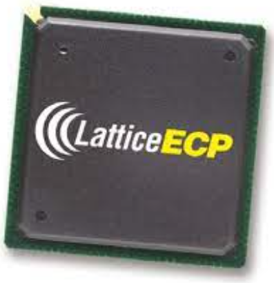
Description
The LatticeECP/EC family of FPGA devices is designed to provide common FPGA functionalities at a reasonable price. The LatticeECP (EConomy Plus) FPGA idea combines an effective FPGA fabric with high-speed dedicated functionalities for optimal performance and value. The LatticeECPDSP (EConomy Plus DSP) family is the first family to use this methodology and offers specialized high-performance DSP blocks on-chip. To achieve more affordable solutions, the LatticeEC (EConomy) family provides all the general-purpose characteristics of LatticeECP devices without specialized function blocks. All essential FPGA components are present in the LatticeECP/EC FPGA fabric, which was created with low cost in mind from the beginning. These components include LUT-based logic, distributed and embedded memory, PLLs, and support for common I/Os. Additionally included is dedicated DDR memory interface logic, which is becoming more and more common in applications with tight budgets. Large complicated designs can be effectively implemented using the LatticeECP/EC FPGA family thanks to the ispLEVER design tool package from Lattice. Popular logic synthesis tools include support for LatticeECP/EC synthesis libraries. The ispLEVER tool places and routes the design in the LatticeECP/EC device using the output from the synthesis tool and the limitations from its floor planning tools. For timing verification, the ispLEVER tool takes the timing from the routing and back-annotates it into the design. For the LatticeECP/EC family, Lattice offers a wide variety of pre-designed IP (Intellectual Property) ispLeverCORE modules. Designers can focus on the distinctive elements of their designs while still employing these IPs as standardized building blocks, which increases productivity.
Features
Extensive Density and Package Options
• 1.5K to 32.8K LUT4s
• 65 to 496 I/Os
• Density migration supported
sysDSP Block (LatticeECP Versions)
• High performance multiply and accumulate
• 4 to 8 blocks
4 to 8 36x36 multipliers or
– 16 to 32 18x18 multipliers or
32 to 64 9x9 multipliers
Embedded and Distributed Memory
• 18 Kbits to 498 Kbits sysMEM Embedded Block RAM (EBR)
• Up to 131 Kbits distributed RAM
• Flexible memory resources:
Distributed and block memory
Flexible I/O Buffer
• Programmable sysI/O buffer supports wide range of interfaces:
LVCMOS 3.3/2.5/1.8/1.5/1.2
LVTTL
SSTL 3/2 Class I, II, SSTL18 Class I
HSTL 18 Class I, II, III, HSTL15 Class I, III
PCI
LVDS, Bus-LVDS, LVPECL, RSDS
Dedicated DDR Memory Support
• Implements interface up to DDR400 (200MHz)
sysCLOCK PLLs
• Up to four analog PLLs per device
• Clock multiply, divide and phase shifting
System Level Support
• IEEE Standard 1149.1 Boundary Scan, plus ispTRACY internal logic analyzer capability
• SPI boot flash interface
• 1.2V power supply
Low Cost FPGA
• Features optimized for mainstream applications
• Low cost TQFP and PQFP packaging
