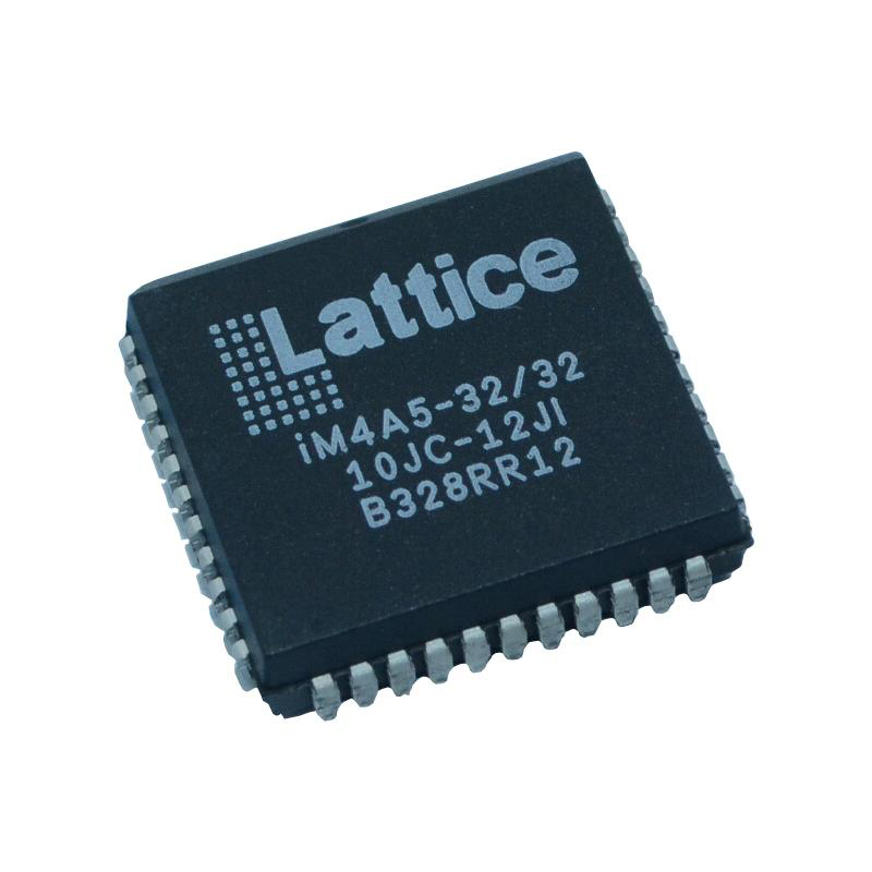
The flexiFLASH architecture used by LatticeXP2 devices combines a Look-up Table (LUT) based FPGA fabric with non-volatile Flash cells. Instant-on, limitless reconfigurability, on-chip storage with FlashBAK integrated block memory and Serial TAG memory, as well as design security, are advantages of the flexiFLASH technology. The components also enable 128-bit AES Encryption, Live Update with TransFR, and Dual-boot technologies.
High performance and low cost were priorities when developing the LatticeXP2 FPGA fabric for the new technology. Phase Locked Loops (PLLs), pre-engineered source synchronous I/O support, distributed and embedded memory, LUT-based logic, and improved sysDSP blocks are all features of LatticeXP2 devices. Using the LatticeXP2 series of FPGA devices, big and complicated designs may be efficiently implemented thanks to Lattice Diamond design software. Popular logic synthesis tools can support LatticeXP2 synthesis libraries. The Diamond software places and routes the design in the LatticeXP2 device using the output from the synthesis tool and the limitations from its floor planning tools.
For timing verification, the Diamond tool pulls the timing from the routing and back-annotates it into the design. For the LatticeXP2 family, Lattice offers a wide variety of LatticeCORE pre-designed Intellectual Property (IP) modules. Designers are able to concentrate on the distinctive elements of their designs, enhancing productivity, by employing these IPs as standardized building blocks.
Features
flexiFLASH Architecture
• Instant-on
• Infinitely reconfigurable
• Single chip
• FlashBAK technology
• Serial TAG memory
• Design security
Live Update Technology
• TransFR technology
• Secure updates with 128 bit AES encryption
• Dual-boot with external SPI
sysDSP Block
• Three to eight blocks for high performance
Multiply and Accumulate
• 12 to 32 18x18 multipliers
• Each block supports one 36x36 multiplier or four 18x18 or eight 9x9 multipliers
Embedded and Distributed Memory
• Up to 885 Kbits sysMEM EBR
• Up to 83 Kbits Distributed RAM
sysCLOCK PLLs
• Up to four analog PLLs per device
• Clock multiply, divide and phase shifting
Flexible I/O Buffer
• sysIO buffer supports:
– LVCMOS 33/25/18/15/12; LVTTL
– SSTL 33/25/18 class I, II
– HSTL15 class I; HSTL18 class I, II
– PCI
– LVDS, Bus-LVDS, MLVDS, LVPECL, RSDS
Pre-engineered Source Synchronous Interfaces
• DDR / DDR2 interfaces up to 200 MHz
• 7:1 LVDS interfaces support display applications
• XGMII
Density And Package Options
• 5k to 40k LUT4s, 86 to 540 I/Os
• csBGA, TQFP, PQFP, ftBGA and fpBGA packages
• Density migration supported
Flexible Device Configuration
• SPI (master and slave) Boot Flash Interface
• Dual Boot Image supported
• Soft Error Detect (SED) macro embedded
System Level Support
• IEEE 1149.1 and IEEE 1532 Compliant
• On-chip oscillator for initialization & general use
• Devices operate with 1.2V power supply
