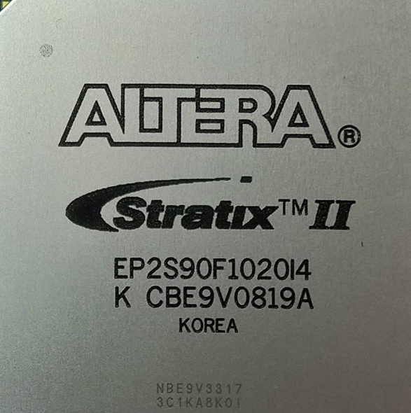
The Stratix II FPGA family uses a novel logic topology to maximize performance and enable device densities up to 180,000 equivalent logic elements (LEs). It is based on a 1.2-V, 90-nm, all-layer copper SRAM process. allowing demanding, memory-intensive applications, Stratix II devices provide up to 9 Mbits of on-chip TriMatrix memory. They also have up to 96 DSP blocks with up to 384 (18-bit 18-bit) multipliers allowing effective implementation of high performance filters and other DSP operations. There are several high-speed external memory interfaces that are supported, including single data rate (SDR) SDRAM, quad data rate (QDR) II SRAM, RLDRAM II, and double data rate (DDR) and DDR2 SDRAM. Stratix II devices support various I/O standards along with support for 1-gigabit per second (Gbps) source synchronous signaling with DPA circuitry.
With an internal clock frequency of up to 550 MHz and up to 12 phase-locked loops (PLLs), Stratix II devices provide a comprehensive clock management solution. Additionally, Stratix II devices are the first FPGAs in the market to be able to decrypt a configuration bitstream that has been encrypted with the Advanced Encryption Standard (AES) technique to safeguard designs.
