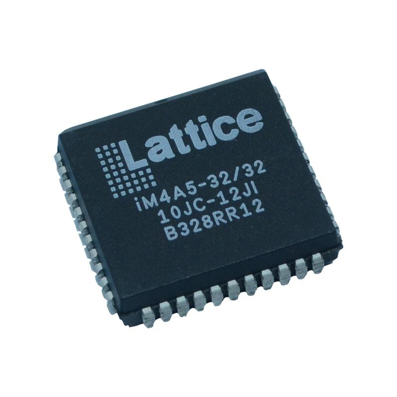
Description
The LatticeECP2/M series of FPGA devices are designed to give high-performance capabilities including sophisticated DSP blocks, high-speed SERDES (LatticeECP2M family only), and high-speed source synchronous interfaces in a budget-friendly FPGA fabric. This combination was made possible by 90nm technology and improvements in device architecture. High performance and low cost are priorities when designing the LatticeECP2/M FPGA fabric. The LatticeECP2/M devices feature encryption ("S" versions only) and dual boot capabilities, as well as LUT-based logic, distributed and embedded memory, Phase Locked Loops (PLLs), Delay Locked Loops (DLLs), pre-engineered source synchronous I/O support, and enhanced sysDSP blocks. High-speed SERDES with PCS are a feature of the LatticeECP2M device family. These SERDES with PCS blocks, which have high jitter tolerance and low transmission jitter, can be set up to handle a variety of well-liked data protocols, including PCI Express, Ethernet (1GbE and SGMII), OBSAI, and CPRI. Chip to chip and small form factor backplane applications are well suited for SERDES thanks to its transmit pre-emphasis and receive equalization settings. Large complicated designs can be efficiently built using the LatticeECP2/M FPGA family thanks to Lattice Diamond design software. Popular logic synthesis tools include support for LatticeECP2/M synthesis libraries. The Diamond software places and routes the design in the LatticeECP2/M device using the output from the synthesis tool and the limitations from its floor planning tools. For timing verification, the Diamond design tool pulls the timing from the routing and back-annotates it into the design. For the LatticeECP2/M family, Lattice offers a wide variety of pre-engineered IP (Intellectual Property) modules. Because these IP cores serve as standardized building blocks, designers are free to focus on the distinctive features of their designs, which boosts productivity.
Features
High Logic Density for System Integration
• 6K to 95K LUTs
• 90 to 583 I/Os
Embedded SERDES (LatticeECP2M Only)
• Data Rates 250 Mbps to 3.125 Gbps
• Up to 16 channels per device PCI Express, Ethernet (1GbE, SGMII), OBSAI, CPRI and Serial RapidIO.
sysDSP Block
• 3 to 42 blocks for high performance multiply and accumulate
• Each block supports
– One 36x36, four 18x18 or eight 9x9 multipliers
Flexible Memory Resources
• 55Kbits to 5308Kbits sysMEM Embedded Block RAM (EBR)
– 18Kbit block
– Single, pseudo dual and true dual port
– Byte Enable Mode support
• 12K to 202Kbits distributed RAM
– Single port and pseudo dual port
sysCLOCK Analog PLLs and DLLs
• Two GPLLs and up to six SPLLs per device
– Clock multiply, divide, phase & delay adjust
– Dynamic PLL adjustment
• Two general purpose DLLs per device
Pre-Engineered Source Synchronous I/O
• DDR registers in I/O cells
• Dedicated gearing logic
• Source synchronous standards support
– SPI4.2, SFI4 (DDR Mode), XGMII
– High Speed ADC/DAC devices
• Dedicated DDR and DDR2 memory support
– DDR1: 400 (200MHz) / DDR2: 533 (266MHz)
• Dedicated DQS support
Programmable sysI/O Buffer Supports Wide Range Of Interfaces
• LVTTL and LVCMOS 33/25/18/15/12
• SSTL 3/2/18 I, II
• HSTL15 I and HSTL18 I, II
• PCI and Differential HSTL, SSTL
• LVDS, RSDS, Bus-LVDS, MLVDS, LVPECL
Flexible Device Configuration
• 1149.1 Boundary Scan compliant
• Dedicated bank for configuration I/Os
• SPI boot flash interface
• Dual boot images supported
• TransFR I/O for simple field updates
• Soft Error Detect macro embedded
Optional Bitstream Encryption
(LatticeECP2/M “S” Versions Only)
System Level Support
• ispTRACY internal logic analyzer capability
• On-chip oscillator for initialization & general use
• 1.2V power supply
