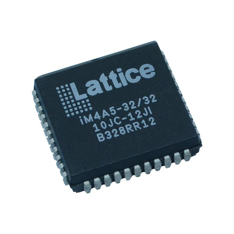
The MachXO3D family, which has improved security features and on-chip dual boot flash, is the next generation of Lattice Semiconductor Low Density PLDs. AES-128/256, Secure Hash Algorithm (SHA)-256, Elliptic Curve Digital Signature Algorithm (ECDSA), Elliptic Curve Integrated Encryption Scheme (ECIES), Hash Message Authentication Code (HMAC)-SHA256, Public Key Cryptography, and Unique Secure ID are some of the improved security features. The MachXO3D family is a Root-of-Trust hardware solution that, thanks to its improved bitstream security and user mode features, can easily expand to secure the entire system.
The MachXO3D offers unprecedented I/O density and a large variety of I/O programmability choices. The device's I/O includes compatibility for the most recent industry standards, including as I3C and configurable slew rates. There are two low power, Flash-based PLDs in the MachXO3D family that have densities of 4300 and 9400 Look-Up Tables (LUTs). On-chip dual boot configuration flash and multi-sectored User Flash Memory (UFM) are also features of MachXO3D devices. These devices include LUT-based programmable logic in addition to embedded block RAM (EBR), distributed RAM, locked loops (PLLs), pre-engineered source synchronous I/O support, advanced configuration support including on-chip dual-boot capability, and hardened variations of frequently used features like the SPI controller, the I2C controller, and the timer/counter.
MachXO3D are built using a non-volatile, low power 65-nm technology. The architecture of the device contains a number of characteristics, including programmable low swing differential I/O and the capacity to dynamically disable I/O banks, on-chip PLLs, and oscillators. These functions aid in controlling static and dynamic power consumption, resulting in minimal power usage for all family members.
Features
1.1.1. Solutions
Best-In-Class control PLD with advanced security
functions, provide secure/authenticated boot and
root of trust function
Optimized footprint, logic density, I/O count, I/O
performance devices for I/O management and
logic applications
High I/O logic, high I/O devices for I/O expansion
applications
1.1.2. Flexible Architecture
Logic Density ranging from 4.3K to 9.4K LUT4
High I/O to LUT ratio with up to 383 I/O pins
1.1.3. Dedicated Embedded Security Block
Advanced Encryption Standard (AES): AES-128/256 Encryption/Decryption
Secure Hash Algorithm (SHA): SHA-256
Elliptic Curve Digital Signature Algorithm (ECDSA): ECDSA-based authentication
Hash Message Authentication Code (HMAC): HMAC-SHA256
Elliptic Curve Integrated Encryption Scheme (ECIES): ECIES Encryption and Decryption
True Random Number Generator (TRNG)
Key Management using Elliptic Curve DiffieHellman (ECDH) Public Key Cryptography
Unique Secure ID
Guard against malicious attacks
Interface for user logic via WISHBONE and High Speed Port (HSP)
Federal Information Processing Standard (FIPS) supported Security Protocols
1.1.4. Pre-Engineered Source Synchronous I/O
DDR registers in I/O cells
Dedicated gearing logic
7:1 Gearing for Display I/O
Generic DDR, DDRx2, DDRx4 1.1.5. High Performance, Flexible I/O Buffer
Programmable sysI/OTM buffer supports wide range of interfaces:
LVCMOS 3.3/2.5/1.8/1.5/1.2
LVTTL
LVDS, Bus-LVDS, MLVDS, LVPECL
MIPI D-PHY Emulated
Schmitt trigger inputs, up to 0.5 V hysteresis
Ideal for I/O bridging applications
I3C compatible on selective I/O
Slew rate control as Slow/Fast
I/O support hot socketing
On-chip differential termination
Programmable pull-up or pull-down mode
1.1.6. Flexible On-Chip Clocking
Eight primary clocks
Up to two edge clocks for high-speed I/O interfaces (top and bottom sides only)
Two analog PLLs per device with fractional-n frequency synthesis
Wide input frequency range (7 MHz to 400 MHz).
1.1.7. Non-volatile, Reconfigurable
Instant-on
Powers up in microseconds
On-chip dual boot
Multi-sectored UFM for customer data storage
Single-chip, secure solution
Programmable through JTAG, SPI or I2C
Reconfigurable Flash
Supports background programming of non-volatile memory
1.1.8. TransFR Reconfiguration
In-field logic update while I/O holds the system state
1.1.9. Enhanced System Level Support
On-chip hardened functions: SPI, I2C, and timer/counter
On-chip oscillator with 5.5% accuracy
Unique TraceID for system tracking
Single power supply with extended operating range
IEEE Standard 1149.1 boundary scan
IEEE 1532 compliant in-system programming
1.1.10. Advanced Packaging
0.5 mm pitch: 4.3K to 9.4K densities with up to 58 I/O in QFN packages
0.8 mm pitch: 4.3K to 9.4K densities with up to 383 I/O in BGA packages
Pin-compatible with MachXO3LF product family of devices
1.1.11. Applications
Secure boot and Root of Trust
Consumer Electronics
Compute and Storage
Wireless Communications
Industrial Control Systems
Automotive System
