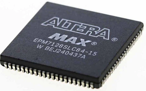
The revolutionary MAX® V CPLD design consists of a wide variety of logic elements (LEs grouped in logic array blocks (LABs)), memory resources (non-volatile flash and LE RAM), global signals (clocks or control signals), and a sizable number of user I/Os. The most effective, direct link from input to logic to output is used in the MultiTrack interconnect to maximize performance and reduce power consumption.
In collaboration with Quartus Prime Software
The MAX® V CPLD architecture and Quartus® Prime software fitting methods were improved together to maximize tPD, tCO, tSU, and fMAX performance with pins locked down. This simplified the design optimization process. Quartus Prime software uses locked pin assignments and a push-button compilation sequence to improve the ability to meet or surpass performance requirements when design functionality changes. The free Quartus® Prime Lite Edition software is compatible with all MAX® V CPLDs.
Voltage Flexibility for I/O
The MAX® V CPLD design provides MultiVolt I/O capabilities, which enables various I/O banks to function with various I/O voltages and link to other devices without any issues. A single 1.8-V external supply (VCCINT) powers the device core, enabling CPLD operation with minimal dynamic and standby power. The bigger density products have four I/O banks compared to the smaller density devices' two. Each bank may get a separate VCCIO reference voltage supply.
