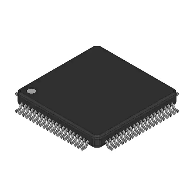
In-system programmable configuration PROMs from Xilinx are now available in the XC18V00 series. These 3.3V devices, which include a 4-megabit, 2-megabit, 1-megabit, and 512-kilobit PROM, offer a simple, affordable way to reprogramme and store Xilinx FPGA configuration bitstreams.
The PROM is driven by a configuration clock that the FPGA creates when it is operating in Master Serial mode. Data is accessible on the PROM DATA (D0) pin, which is coupled to the FPGA DIN pin, after a brief access time after CE and OE are enabled. After each rising clock edge, fresh data becomes accessible for a brief period of time. The right number of clock pulses are produced by the FPGA to finish the configuration. When the FPGA is in Slave Serial mode, the PROM and the FPGA are clocked by an external clock.
The FPGA produces a configuration clock that drives the PROM when it is operating in Master SelectMAP mode. The configuration clock that powers the PROM and the FPGA is produced by an external oscillator when the FPGA is operating in Slave Parallel or Slave SelectMAP mode. Data is accessible on the PROM's DATA (D0-D7) pins once CE and OE have been enabled. After each rising clock edge, fresh data becomes accessible for a brief period of time. On the CCLK's subsequent rising edge, the data is clock into the FPGA. In the Slave Parallel or Slave SelecMAP modes, a free-running oscillator may be utilized.
By driving the CE input of the next device with the CEO output, multiple devices can be cascaded. All the PROMs in this chain's clock inputs and DATA outputs are connected. Each device works with the others in the family as well as the XC17V00 one-time programmable serial PROM family and can be cascaded.
