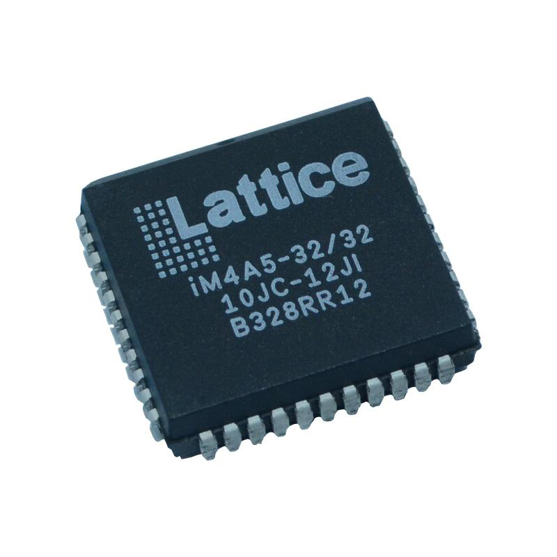
An assortment of logic blocks are surrounded by programmable I/O (PIO) in the LCMXO1200LUTSC-5TN100I architecture. SysCLOCK PLLs and blocks of sysMEM Embedded Block RAM (EBRs) are present in some of the devices in devices. The block schematics of the different {} members are displayed in Figures 2-1, 2-2, and 2-3. A two-dimensional grid with rows and columns holds the logic blocks. To the left of the logic array, a column of EBR blocks is organized. The PIO cells are grouped into Banks and are situated on the device's edge. A flexible I/O buffer used by the PIOs is known as a sysIO interface, and it allows for operation with a number of different interface standards. Numerous vertical and horizontal routing channel resources connect the blocks. These routing resources are automatically distributed using the put and route software program. The Programmable Functional Unit (PFU) and the Programmable Functional Unit without RAM (PFF) are the two different types of logic blocks. The foundational elements for logic, arithmetic, RAM, ROM, and register functions are found in the PFU. Building blocks for logic, arithmetic, ROM, and register functions are found in the PFF block. Due to the versatility of the PFU and PFF blocks, complicated designs can be realized fast and successfully. In a two-dimensional array, logic building units are grouped. Per row, only one kind of block is utilized. Each device in the MachXO series has a different number of sysIO Banks. On various Banks, there are many I/O Buffer types. See the specifics in this document's subsequent parts. The sysMEM EBRs are substantial, fast memory blocks that are only present in larger devices. These blocks can be set up as FIFO, ROM, or RAM. To reduce the need for LUTs, FIFO support contains separate FIFO pointer and flag "hard" control logic. Both SET and RESET configurations are available for the MachXO registers in PFU and sysI/O. The device enters user mode with these registers set or reset in accordance with the configuration settings after being powered on, enabling the device to enter a known state for predictable system function. On bigger devices, the MachXO design offers up to two sysCLOCK Phase Locked Loop (PLL) blocks. The memory blocks have these blocks at their ends. The frequency and phase relationships of the clocks are managed using the PLLs' multiply, divide, and phase-shifting capabilities. Every LCMXO1200LUTSC-5TN100I has a JTAG Port that allows access to the user logic as well as programming and configuration of the device. The MachXO devices are simple to integrate into the entire system because they can operate from 3.3 V, 2.5 V, 1.8 V, and 1.2 V power supply.
Buy LCMXO1200E-3MN132I Lattice Semiconductor, Get familiar with the LCMXO1200E-3MN132I MachXO Family...
Buy LCMXO1200E-3MN132C Lattice Semiconductor, Get familiar with the LCMXO1200E-3MN132C MachXO Family...
Buy LCMXO1200E-3M132I Lattice Semiconductor, Get familiar with the LCMXO1200E-3M132I MachXO Family a...
Buy LCMXO1200E-3M132C Lattice Semiconductor, Get familiar with the LCMXO1200E-3M132C MachXO Family a...
Buy LCMXO1200E-3FTN256I Lattice Semiconductor, Get familiar with the LCMXO1200E-3FTN256I MachXO Fami...