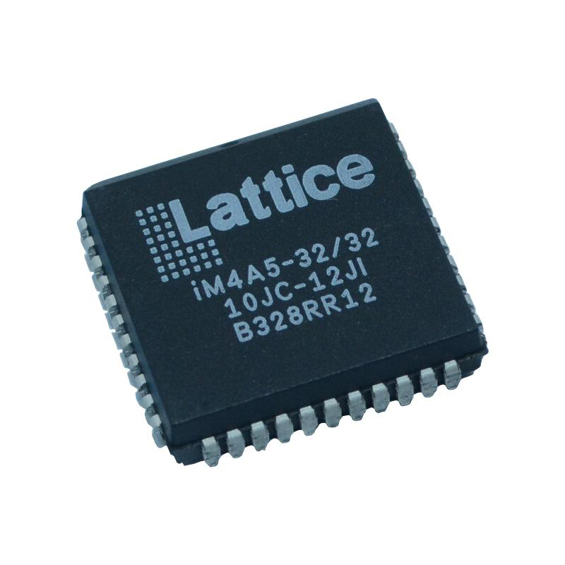

A few of the high-performance features that the LFSCM3GA15EP1-6FN900C is designed to provide in a cheap FPGA fabric include a high-performance DSP architecture, high-speed SERDES (Serializer/Deserializer), and high-speed source synchronous interfaces. This combination of advances in device architecture and the use of 40 nm technology makes the devices suitable for high-volume, high-speed, and low-cost applications. LFSCM3GA15EP1-6FN900C has a look-up-table (LUT) capacity of 84K logic components and supports up to 365 users I/O. A high-performance DSP architecture, high-speed SERDES (Serializer/Deserializer), and high-speed source synchronous interfaces are just a few of the high-performance characteristics that LFSCM3GA15EP1-6FN900C is intended to offer in a low-cost FPGA fabric. The utilization of 40 nm technology in conjunction with improvements in device architecture makes the devices appropriate for high-volume, high-speed, and low-cost applications. LFSCM3GA15EP1-6FN900C supports up to 365 user I/O and has a look-up-table (LUT) capacity of 84K logic components.
The pre-engineered source synchronous logic of LFSCM3GA15EP1-6FN900C supports a broad range of interface protocols, including DDR2/3, LPDDR2/3, XGMII, and 7:1 LVDS. Another component of LFSCM3GA15EP1-6FN900C is high-speed SERDES with particular Physical Coding Sublayer (PCS) features. Due to their high jitter tolerance and low transmit jitter, the SERDES plus PCS blocks can be used to support a number of popular data protocols, such as PCI Express, Ethernet (XAUI, GbE, and SGMII), and CPRI. The SERDES's Receive Equalization settings and Transmit De-emphasis with pre- and post-cursors make it suitable for transmission and reception via a range of media. Along with bit-stream encryption, dual boot support, and TransFR field upgrading features, LFSCM3GA15EP1-6FN900C also provides flexible, trustworthy, and secure configuration options. LFSCM3GA15EP1-6FN900C has improved in the SERDES as compared to ECP5UM devices. The SERDES can now run at up to 5 Gb/s of data rate thanks to these upgrades.
Pin-to-pin compatibility exists between the ECP5UM product and devices from the LFSCM3GA15EP1-6FN900C. These allow you to transfer designs for devices with better performance from ECP5UM to ECP5-5G products. The Lattice Diamond design software enables efficient implementation of large complex designs using LFSCM3GA15EP1-6FN900C. Support for synthesis libraries for LFSCM3GA15EP1-6FN900C is available in popular logic synthesis tools. Diamond tools use the output from the synthesis tool and the constraints from its floor planning tools to install and route the design in the ECP5/ECP5-5G device. The tools take the time from the routing and back-annotate it into the design for timing verification.
Lattice provides a range of pre-engineered IP (Intellectual Property) modules for LFSCM3GA15EP1-6FN900C. When using these flexible soft-core IPs as standardized building blocks, designers have more freedom to concentrate on the unique aspects of their designs, which increases productivity.
| Specification | Value |
|---|---|
| Number of I/Os | 132 to 942 |
| Operating Supply Voltage | 1.2 V |
| Maximum Operating Temperature | + 85℃ |
| Mounting Style | SMD/SMT |
| Package / Case | FPBGA-900 |
| Minimum Operating Temperature | 0 C |
| Packaging | Tray |
| Factory Pack Quantity | 135 |

Buy LFSC3GA25E-6FFA1020C Lattice Semiconductor, Get familiar with the LFSC3GA25E-6FFA1020C LatticeSC...

Buy LFSC3GA25E-6F900I Lattice Semiconductor, Get familiar with the LFSC3GA25E-6F900I LatticeSC/M Fam...

Buy LFSC3GA25E-6F900C-5I Lattice Semiconductor, Get familiar with the LFSC3GA25E-6F900C-5I LatticeSC...

Buy LFSC3GA25E-5FFAN1020C Lattice Semiconductor, Get familiar with the LFSC3GA25E-5FFAN1020C Lattice...

Buy LFSC3GA25E-5FFA1020I Lattice Semiconductor, Get familiar with the LFSC3GA25E-5FFA1020I LatticeSC...