In the LFXP3E-5T100C-4I design, Programmable I/O Cells (PIC) encircle an array of logic blocks. Rows of sysMEM Embedded Block RAM (EBR) are interspersed between the rows of logic blocks. Non-volatile Memory Blocks are located on the left and right sides of the PFU array. This nonvolatile memory is configured using either the sysCONFIG peripheral port or the IEEE 1149.1 TAP port. The configuration information is moved from the Non-Volatile Memory Blocks to the configuration SRAM at power-up. This solution eliminates the need for pricey external configuration memories and protects designs from illegal read-back. The data is transferred in microseconds from non-volatile memory to configuration SRAM through wide busses, offering a "instant-on" feature that makes interfacing in many applications simple. The Programmable Functional Unit (PFU) and the Programmable Functional Unit without RAM/ROM (PFF) are the two different types of logic blocks. The foundational elements for logic, arithmetic, RAM, ROM, and register functions are found in the PFU. Building blocks for logical, mathematical, and ROM functions are found in the PFF block. Due to the versatility of PFU and PFF blocks, complicated designs can be realized rapidly and effectively. An array of Logic Blocks is set up in two dimensions. Per row, only one kind of block is utilized. The outer rows are constructed with PFU blocks. Rows of PFF blocks and rows of PFU blocks make up the remaining portion of the core. A row of PFU blocks is present for every three rows of PFF blocks. Two PIOs (PIO pairs) with corresponding sysIO interfaces make up each PIC block. PIO pairs on the device's left and right edges may be set up as transmit/receive LVDS pairs. Large dedicated fast memory blocks known as sysMEM EBRs. They can be set up to function as ROM or RAM. Numerous vertical and horizontal routing channel resources connect the blocks. These routing resources are automatically distributed using the put and route software program. The sysCLOCK Phase Locked Loop (PLL) Blocks are located at the end of the rows holding the sysMEM Blocks. These PLLs, which have the capacity to multiply, divide, and phase shift, are used to control the phase connection between the clocks. Up to four PLLs are available per device using the LFXP3E-5T100C-4I design. A JTAG Port with internal Logic Analyzer (ispTRACY) capabilities is present on every member of the LFXP3E-5T100C-4I of devices. Device configuration for serial or parallel devices is possible using the sysCONFIG port. The LFXP3E-5T100C-4I devices are simple to integrate into the overall system because they can operate from 3.3V, 2.5V, 1.8V, and 1.2V power supply.
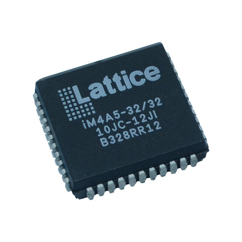
Buy LFXP10EB-03FN256C Lattice Semiconductor, Get familiar with the LFXP10EB-03FN256C LatticeXP Famil...

Buy LFXP10E-5FTN256C-4I Lattice Semiconductor, Get familiar with the LFXP10E-5FTN256C-4I LatticeXP F...

Buy LFXP10E-5FN388C Lattice Semiconductor, Get familiar with the LFXP10E-5FN388C LatticeXP Family at...

Buy LFXP10E-5FN256C-4I Lattice Semiconductor, Get familiar with the LFXP10E-5FN256C-4I LatticeXP Fam...

Buy LFXP10E5FN256C-4I Lattice Semiconductor, Get familiar with the LFXP10E5FN256C-4I LatticeXP Famil...