GENERAL DESCRIPTION
An improved PAL device called the PALCE16V8H-30E4/BRA was created using low-power, high-speed, electrically erasable CMOS technology. All 20-pin GAL devices are functionally compatible with it. A ubiquitous device architecture is provided by the macrocells. With the exception of the PAL16C1, the PALCE16V8H-30E4/BRA will directly replace the PAL16R8. The PALCE16V8H-30E4/BRA offers high speed and no standby power. The PALCE16V8H-30E4/BRA enables prolonged battery-powered operation with a maximum standby current of 30 A. The PALCE16V8H-30E4/BRA employs the well-known sum-of-products (AND/OR) architecture, allowing users to quickly and effectively design complex logic operations. Combinatorial logic at several levels can always be converted to sum-of-products form by making use of the extremely wide input gates included in PAL devices. Through electrically erasable floating-gate cells in the AND logic array, the equations are encoded into the gadget. For logic functions, the fixed OR array permits up to eight data product terms per output. The output macrocell is fed by the aggregate of these products. Each macrocell has a registered or combinatorial active-high or active-low output that can be configured. Four multiplexers are controlled by two global bits and one local bit in each macrocell, which decide the output configuration.
FUNCTION DESCRIPTION
The PALCE16V8H-30E4/BRA is an all-purpose PAL gadget. The zero-power variant of the PALCE16V8H-30E4/BRA is the PALCE16V8H-30E4/BRA. It has all the PALCE16V8H-30E4/BRA's architectural elements. The PALCE16V8H-30E4/BRA also includes zero standby power and a power-saving function called unneeded product term disable. Eight independently programmable macrocells (MC0-MC7) make up this device. Each macrocell can be set up as a dedicated input, registered output, combinatorial output, or combinatorial I/O. A fixed OR logic array is driven by a programmable AND logic array that is implemented in the programming matrix. In order to enable user-programmable input signal polarity, buffers for device inputs include complimentary outputs. For all flip-flops, pins 1 and 11 are either used as array inputs or as the clock (CLK) and output enable (OE), respectively. Unused input pins ought to be connected directly to GND or VCC. Product terms with both the true and complement of any input signal connected assume a logical LOW state, while product terms with all bits unprogrammed (disconnected) assume the logical HIGH state. The user's design specification is automatically used to configure the programmable features on the PALCE16V8H-30E4/BRA. Development software processes the design specification to validate the design and generate a programming file (JEDEC). When this file is downloaded to a programmer, the device is configured to perform the user's intended function. The PALCE16V8H-30E4/BRA offers the customer two design possibilities. It can first be set up as a PAL16R8 series regular PAL device. Device codes for the PALCE16V8H-30E4/BRA's compatible standard PAL device architectures will be provided by the PAL programmer manufacturer. The PALCE16V8H-30E4/BRA will be programmed in the appropriate architecture by the programmer. By doing this, the user can use the JEDEC files for conventional PAL devices without altering them.The device can also be set up to function as a PALCE16V8H-30E4/BRA. The PALCE16V8H-30E4/BRA device code must be entered in this case. The macrocell may be used entirely with this choice.
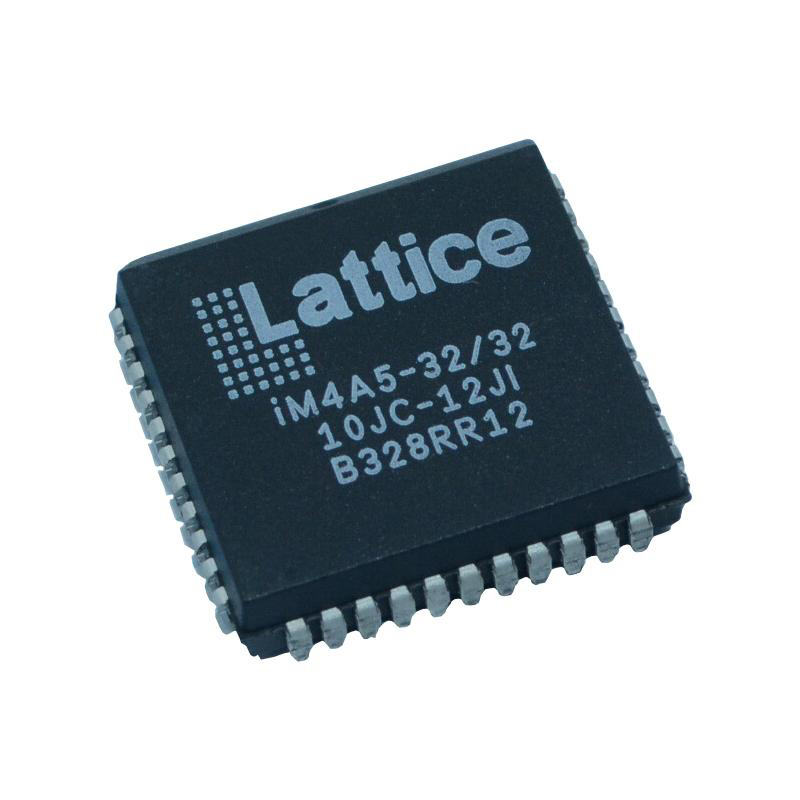
Buy PALCE16V8H10JC4 Lattice Semiconductor, Get familiar with the PALCE16V8H10JC4 PALCE16V8 Family at...

Buy PALCE16V8H-10/15 Lattice Semiconductor, Get familiar with the PALCE16V8H-10/15 PALCE16V8 Family ...

Buy PALCE16V8A-15SC Lattice Semiconductor, Get familiar with the PALCE16V8A-15SC PALCE16V8 Family at...

Buy PALCE16V8A-10 Lattice Semiconductor, Get familiar with the PALCE16V8A-10 PALCE16V8 Family at VEK...

Buy PALCE16V8-7PC/4 Lattice Semiconductor, Get familiar with the PALCE16V8-7PC/4 PALCE16V8 Family at...