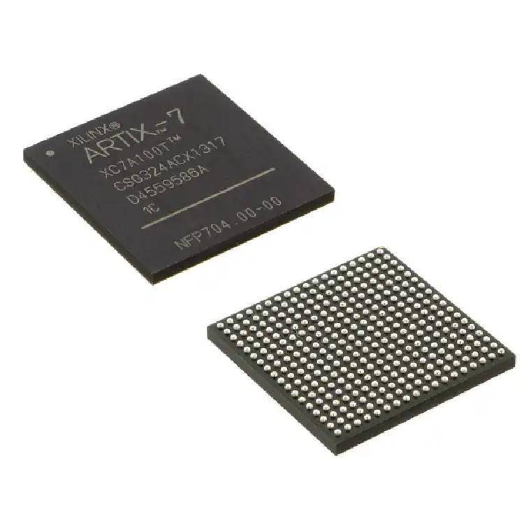
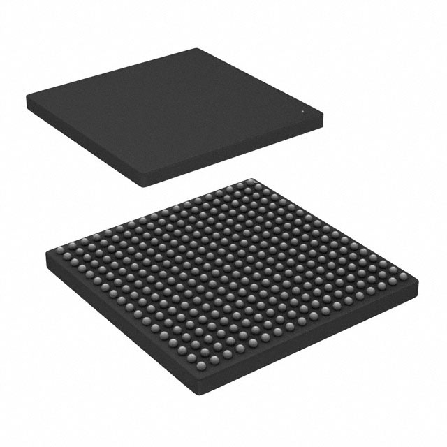
XC7A50T-L2FTG256E are contained in the FBGA package. This kind of FPGA's component is called FIELD PROGRAMMABLE GATE ARRAY. It transfers data more effectively thanks to its 170 I/Os. 52160 logic components/cells make up a basic building block. A 0.9V-volt supply serves as the source of power. This component is a member of the FPGA family known as Field Programmable Gate Arrays. This kind of equipment has 170 built-in outputs. With 256 terminations, Fpga chips are designed. This FPGA module has a maximum RAM size of 337.5kB, which is required to guarantee the smooth running of the software. 256 pins have been created in order to make it function. If put in Surface Mount, this FPGA might, in my opinion, give excellent results if its parameters are followed. Designers may fully utilize the versatility of the device when operating at 900mV. A 0.9V power source is needed by fpga circuits in order for them to function. The maximum temperature at which this module can function is 100 °C. It is advised that the working temperature for fpga electronics be higher than 0°C. I'm going to show you a gadget that has 256 pins on it. This system's fundamental building block is made up of 4075 logic blocks (LABs). Typically, a 1098MHz crystal is used in fpga semiconductor. There are 65200 registers in use in total for data storage and transport. Another name for this feature is ALSO OPERATES AT 1V SUPPLY, which is one of its key attributes. View Substitutes & Alternatives, datasheets, stock, pricing from Authorized Distributors, as well as other FPGAs goods, at www.vemeko.com.
MicroBlaze™ processor: The MicroBlaze™ processor is a soft processor that can be used to quickly deploy embedded processing.
36 Kb dual-port block RAM: The 36 Kb dual-port block RAM has integrated FIFO circuitry for on-chip data buffering.
High-performance SelectIO™ technology: The high-performance SelectIO™ technology supports DDR3 interfaces up to 1,866 Mb/s.
Integrated PCI Express® (PCIe) block: The integrated PCI Express® (PCIe) block supports up to x8 Gen3 Endpoint and Root Port designs.
Powerful clock management tiles (CMT): The powerful clock management tiles (CMT) integrate mixed-mode clock manager (MMCM) and phase-locked loop (PLL) blocks for high precision and minimal jitter.
Dual 12-bit 1MSPS analog-to-digital converters: The dual 12-bit 1MSPS analog-to-digital converters with on-chip supply and heat sensors make up the user-configurable analog interface (XADC).
Medical devices
Defense applications
Industrial
Consumer
Automotive
Any-to-any connectivity
Sensor fusion
Embedded vision
Software defined radio
Programmable logic controller
| Specification | Value |
| Mount | Surface Mount |
| Package / Case | FBGA |
| Number of Pins | 256 |
| JESD-609 Code | e1 |
| Pbfree Code | yes |
| Number of Terminations | 256 |
| Max Operating Temperature | 100°C |
| Min Operating Temperature | 0°C |
| Supply Voltage | 0.9V |
| Terminal Pitch | 1mm |
| Pin Count | 256 |
| Number of Outputs | 170 |
| Operating Supply Voltage | 900mV |
| Supply Voltage-Max (Vsup) | 0.93V |
| Power Supplies | 0.9V |
| Number of I/O | 170 |
| RAM Size | 337.5kB |
| Clock Frequency | 1098MHz |
| Propagation Delay | 850 ps |
| Number of Logic Elements/Cells | 52160 |
| Number of Logic Blocks (LABs) | 4075 |
| Number of Registers | 65200 |

Buy XA7A25T-1CSG325I Xilinx, Inc, Get familiar with the XA7A25T-1CSG325I Artix-7 FPGA at VEKEMO FPGA...
Buy XCAU20P-L1SFVB784I Xilinx, Inc, Get familiar with the XCAU20P-L1SFVB784I Artix-7 FPGA at VEKEMO ...
Buy XCAU20P-2SFVB784I Xilinx, Inc, Get familiar with the XCAU20P-2SFVB784I Artix-7 FPGA at VEKEMO FP...
Buy XC7A12T-L1CPG236I Xilinx, Inc, Get familiar with the XC7A12T-L1CPG236I Artix-7 FPGA at VEKEMO FP...
Buy XC7A12T-3CSG325E Xilinx, Inc, Get familiar with the XC7A12T-3CSG325E Artix-7 FPGA at VEKEMO FPGA...