The PROM is driven by a configuration clock that the XQR17V16CC44M creates when it is operating in Master Serial mode. Data appears on the PROM DATA output pin, which is coupled to the FPGA DIN pin, shortly after the rising clock edge. The right number of clock pulses are produced by the FPGA to finish the configuration. Once set up, it turns off the PROM. When XQR17V16CC44M is in Slave Serial mode, the PROM and the FPGA must both be clocked by an incoming signal.
In Master SelectMAP mode, this device produces the configuration clock that powers both the PROM and the FPGA. On the PROMs DATA (D0-D7) pins, data is available following the rising CCLK edge. On the CCLK's next rising edge, the data will be clock into the FPGA. The PROM and the FPGA need to be both clocked by an incoming signal for the Slave SelectMAP mode of the FPGA to work. The CCLK can be driven by a freerunning oscillator.
By driving the following device's CE input with the CEO output, many devices can be connected together. All the PROMs in this chain's clock inputs and DATA outputs are connected. Each device works with the others and can be cascaded with family members. The FPGA design file is converted into a common Hex format for device programming using either the Xilinx ISE Foundation or ISE WebPACK software, which is then sent to the majority of commercial PROM programmers.
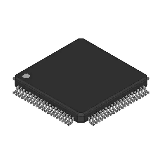
Buy XQR17V16CC44V Xilinx, Inc, Get familiar with the XQR17V16CC44V QPro XQR17V16 series at VEKEMO FP...

Buy XQR17V16VQ44R Xilinx, Inc, Get familiar with the XQR17V16VQ44R QPro XQR17V16 series at VEKEMO FP...

Buy XQR17V16VQ44N Xilinx, Inc, Get familiar with the XQR17V16VQ44N QPro XQR17V16 series at VEKEMO FP...

Buy XQR17V16-CC44V Xilinx, Inc, Get familiar with the XQR17V16-CC44V QPro XQR17V16 series at VEKEMO ...

Buy XQR17V16CC44R Xilinx, Inc, Get familiar with the XQR17V16CC44R QPro XQR17V16 series at VEKEMO FP...