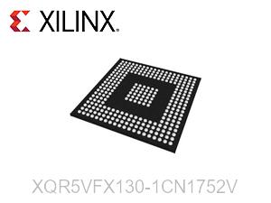
XQR5VFX130-1CN1752V Overview
The XQR5VFX130-1CN1752V is a Virtex-5 FPGA from Xilinx's Virtex-5 family, designed for high-speed, high-density, and highly customizable logic in a wide range of applications, including telecommunications, aerospace, defense, industrial automation, and high-performance computing. With 130,000 logic cells and advanced I/O features, this FPGA offers substantial resources for complex systems that demand rapid processing, flexibility, and scalability.
Key Specifications
- Device Family: Virtex-5 FPGA
- Logic Cells: 130,000 logic cells (LUTs, flip-flops, and multiplexers)
- Package: 1752-pin Fine-Pitch Ball Grid Array (FBGA) (CN1752)
- Voltage Supply: 1.0V (core), 2.5V (I/O)
- Clock Speed: Up to 550 MHz (depending on design complexity and configuration)
- I/O Pins: 832 (max)
- Maximum Power Consumption: 17W (typical), depending on configuration and operating conditions
- Total On-Chip Memory: 1.4 Mb of embedded block RAM (BRAM)
- Embedded Digital Signal Processing (DSP) Slices: 192 DSP slices
- Tolerances: ±5% for voltage supply
- Operating Temperature Range: -40°C to +100°C (industrial grade)
Unique Features and Benefits
- Large Logic Density: The 130,000 logic cells provide ample resources for complex algorithms, signal processing, data management, and embedded systems. Ideal for high-density designs, the Virtex-5 architecture supports advanced routing and logic functions.
- High-Speed Performance: With a clock speed of up to 550 MHz, the XQR5VFX130-1CN1752V can handle complex real-time processing tasks and deliver ultra-low latency, making it suitable for high-speed communications and data-intensive applications.
- Power-Efficient Design: The FPGA operates at a core voltage of 1.0V and provides a power-efficient solution, even in high-performance applications, reducing overall system energy consumption.
- Embedded Memory & DSP: The device includes 1.4 Mb of on-chip block RAM and 192 DSP slices for handling data processing and real-time calculations, enabling efficient signal processing, multimedia applications, and high-performance computing.
- Wide I/O Capability: With 832 I/O pins, the FPGA offers excellent flexibility for interfacing with a variety of external devices and systems, allowing users to build scalable and versatile solutions.
Benefits:
- Customizable Logic: The FPGA allows you to implement custom logic that can be reprogrammed to meet evolving requirements, providing flexibility throughout the lifecycle of your product.
- Enhanced Processing Power: The high logic density and DSP slices make this device ideal for signal processing tasks such as video encoding, encryption, and image processing.
- Efficient System Design: The low power consumption, even at high clock speeds, helps reduce thermal issues and minimizes the need for additional cooling solutions.
Practical Applications & Use Cases
- Telecommunications: The XQR5VFX130-1CN1752V is designed for telecommunication infrastructure, such as high-speed routers, switches, and base stations, where rapid data routing and processing are required.
- Aerospace & Defense: The FPGA’s high performance and rugged reliability make it perfect for aerospace systems, defense electronics, and radar systems where high-density logic, signal processing, and harsh environmental resistance are necessary.
- Industrial Automation: Ideal for industrial control systems, robotics, and embedded computing, the XQR5VFX130-1CN1752V enables efficient real-time data processing and control in factory automation, sensor systems, and machine vision.
- High-Performance Computing (HPC): In data centers and supercomputing systems, this FPGA accelerates computation-intensive tasks like data encryption, machine learning, and artificial intelligence workloads.
- Medical Imaging: The FPGA's high processing power and DSP capabilities make it an excellent choice for medical imaging systems, where real-time image processing and high-speed data transfer are essential.
Problem-Solving Scenarios:
- Real-Time Data Processing: If your application demands real-time signal processing or video encoding/decoding, the high-speed clocking and DSP slices in the XQR5VFX130-1CN1752V provide the necessary resources to handle complex computations without introducing delays.
- Complex Systems with Multiple I/O Requirements: For systems requiring significant I/O bandwidth, the 832 I/O pins enable the FPGA to interface with a variety of external sensors, devices, or processors, while maintaining high-speed communication.
- Power-Constrained Applications: Despite its large logic resources, the XQR5VFX130-1CN1752V’s 1.0V core voltage ensures a power-efficient solution even for demanding applications, such as battery-operated or mobile systems.
Compatibility & Integration
- System Compatibility: The XQR5VFX130-1CN1752V is compatible with a wide range of Xilinx tools, including Vivado Design Suite and ISE Design Suite, which allow for effective FPGA programming, simulation, and configuration. It integrates seamlessly with other Xilinx products and supports high-speed serial transceivers, gigabit Ethernet, and other communication standards.
- Installation: The FPGA comes in a 1752-pin FBGA package, requiring fine-pitch PCB design and assembly techniques for integration. Appropriate assembly equipment and soldering methods are necessary for proper installation.
- Programming: The XQR5VFX130-1CN1752V can be programmed and configured using standard JTAG programming interfaces or through Xilinx's Vivado or ISE tools. The device supports multiple configuration options, including serial and parallel programming modes.
Frequently Asked Questions
What is the core voltage of the XQR5VFX130-1CN1752V?
- The core voltage is 1.0V, while the I/O voltage is 2.5V.
What is the maximum clock speed of this FPGA?
- The XQR5VFX130-1CN1752V can operate at clock speeds up to 550 MHz, depending on the specific design and configuration.
Can this FPGA be used in military and aerospace applications?
- Yes, with its rugged operating temperature range (-40°C to +100°C), it is suitable for use in aerospace, defense, and military systems that require high-performance logic in harsh environments.
How many I/O pins does the XQR5VFX130-1CN1752V have?
- The FPGA has a total of 832 I/O pins, providing extensive connectivity for interfacing with external systems.
What tools are required to program the XQR5VFX130-1CN1752V?
- The FPGA can be programmed using Vivado Design Suite or ISE Design Suite from Xilinx, along with a compatible JTAG programmer.
Troubleshooting Tips
- Configuration Issues: Ensure that the power supply to the FPGA is stable and within the recommended voltage ranges (1.0V core and 2.5V for I/O). Use Xilinx’s Vivado or ISE tools for debugging configuration and programming issues.
- Overheating: Monitor power dissipation closely, especially in high-performance configurations. If the FPGA becomes excessively hot, consider improving heat dissipation through better PCB design or additional cooling mechanisms.
- Slow Performance: If the FPGA is not achieving the expected clock speeds, check the design for timing constraints and optimize the FPGA’s logic and routing to meet performance goals.
Conclusion
The XQR5VFX130-1CN1752V from Xilinx is a powerful, high-performance FPGA designed for applications demanding large-scale logic, fast processing, and high connectivity. Whether used in telecommunications, aerospace, industrial systems, or high-performance computing, the Virtex-5 family FPGA offers flexibility, scalability, and reliability to handle the most complex processing tasks.
XQR5VFX130-1CN1752V Specifications
| Specification | Value |
| Manufacturer. | Xilinx |
| Series | XQR5VFX130 |
| Number of Logic Elements | 131072 LE |
| Adaptive Logic Module - ALM | 20480 ALM |
| Embedded Memory | 10.48 Mbit |
| Number of inputs/outputs | 836 I/O |
| Supply Voltage - Min | 1 V |
| Supply voltage - max | 1 V |
| Minimum Operating Temperature | - 55 C |
| Max. operating temp | + 125 C |
| Data rate | 4.25 Gb/s |
| Number of transceivers | 18 Transceiver |
| Mounting Style | SMD/SMT |
| Package / Case | FPGA-1752 |
| Distributed RAM | 1580 kbit |
| Embedded Block RAM - EBR | 10728 kbit |
| Maximum Operating Frequency | 450 MHz |
| Number of Logic Array Blocks - LAB | 10240 LAB |
| Operating power supply voltage | 1 V |
| Product Type | FPGA - Field Programmable Gate Array |
| Subcategory | Programmable Logic ICs |
| Trademark Name | Virtex |
Application Field
-

Artificial Intelligence
-

5G Technology
-

Cloud Computing
-

Consumer Electronics
-

Wireless Technology
-

Industrial Control
-

Internet of Things
-

Medical Equipment