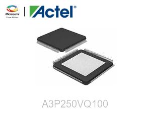
A3P250-VQ100 provides performance, density, and features above and above those of the ProASICPLUS® family. A3P250-VQ100 has the benefit of being a safe, low power, single-chip solution with Instant On thanks to nonvolatile storage technology. This device provides advantages in time to market at ASIC-level unit costs. These properties make it possible for designers to use current ASIC or FPGA design flows and tools to produce high-density systems.
A3P250-VQ100 provides clock conditioning circuitry based on an integrated phase-locked loop (PLL), as well as 1 kbit of on-chip, reprogrammable, nonvolatile FlashROM storage. Both PLL and RAM support are absent from the A3P015 and A3P030 devices. ProASIC3 devices support up to 144 kbits of genuine dual-port SRAM, up to 300 user I/Os, and up to 1 million system gates. ARM Cortex-M1 is supported by ProASIC3 hardware. The Microsemi ordering numbers for the ARM-capable devices start with M1A3P (Cortex-M1) and do not allow AES decryption.
The 130-nm LVCMOS process used by theA3P250-VQ100 provides various advantages, including nonvolatility and reprogrammability. This method is based on advanced flash memory and has seven layers of metal. Logic and control functions are implemented using conventional CMOS design methods. Very high logic usage is possible thanks to the combination of fine granularity, improved flexible routing resources, and numerous flash switches without sacrificing device routability or performance. A four-level routing system within the device connects the logic functions.
Advanced I/O
• 700 Mbps DDR, LVDS-Capable I/Os (A3P250 and above)
• 1.5 V, 1.8 V, 2.5 V, and 3.3 V Mixed-Voltage Operation
• Wide Range Power Supply Voltage Support per JESD8-B, Allowing I/Os to Operate from 2.7 V to 3.6 V
• Bank-Selectable I/O Voltages—up to 4 Banks per Chip
• Single-Ended I/O Standards: LVTTL, LVCMOS 3.3 V /2.5 V / 1.8 V / 1.5 V, 3.3 V PCI / 3.3 V PCI-X† and LVCMOS 2.5 V / 5.0 V Input
• Differential I/O Standards: LVPECL, LVDS, B-LVDS, and M-LVDS (A3P250 and above)
• I/O Registers on Input, Output, and Enable Paths
• Hot-Swappable and Cold Sparing I/Os‡
• Programmable Output Slew Rate† and Drive Strength
• Weak Pull-Up/-Down
• IEEE 1149.1 (JTAG) Boundary Scan Test
• Pin-Compatible Packages across the ProASIC3 Family
High Capacity
• 15 K to 1 M System Gates
• Up to 144 Kbits of True Dual-Port SRAM
• Up to 300 User I/Os
Reprogrammable Flash Technology
• 130-nm, 7-Layer Metal (6 Copper), Flash-Based CMOS
Process
• Instant On Level 0 Support
• Single-Chip Solution
• Retains Programmed Design when Powered Off
High Performance
• 350 MHz System Performance
• 3.3 V, 66 MHz 64-Bit PCI†
• Industrial motor control
• Industrial networking
• Machine vision
• IP and Smart camera
• Video and night vision equipment
| Specification | Value |
| Category | Field Programmable Gate Array |
| Mfr | Microchip Technology |
| Series | ProASIC3 |
| Package | Tray |
| Product Status | Active |
| DigiKey Programmable | Verified |
| Total RAM Bits | 36864 |
| Number of I/O | 68 |
| Number of Gates | 250000 |
| Voltage - Supply | 1.425V ~ 1.575V |
| Mounting Type | Surface Mount |
| Operating Temperature | 0°C ~ 85°C (TJ) |
| Package / Case | 100-TQFP |
| Supplier Device Package | 100-VQFP (14x14) |
| Base Product Number | A3P250 |
Buy A3P1000-PQ208M Actel(Microsemi), Get familiar with the A3P1000-PQ208M FPGA ProASIC3 Families at ...
Buy A3P1000L-FGG256I Actel(Microsemi), Get familiar with the A3P1000L-FGG256I FPGA ProASIC3 Families...
Buy A3P1000-FPQ208 Actel(Microsemi), Get familiar with the A3P1000-FPQ208 FPGA ProASIC3 Families at ...
Buy A3P1000-FGG484 Actel(Microsemi), Get familiar with the A3P1000-FGG484 FPGA ProASIC3 Families at ...
Buy A3P1000-FGG144T Actel(Microsemi), Get familiar with the A3P1000-FGG144T FPGA ProASIC3 Families a...