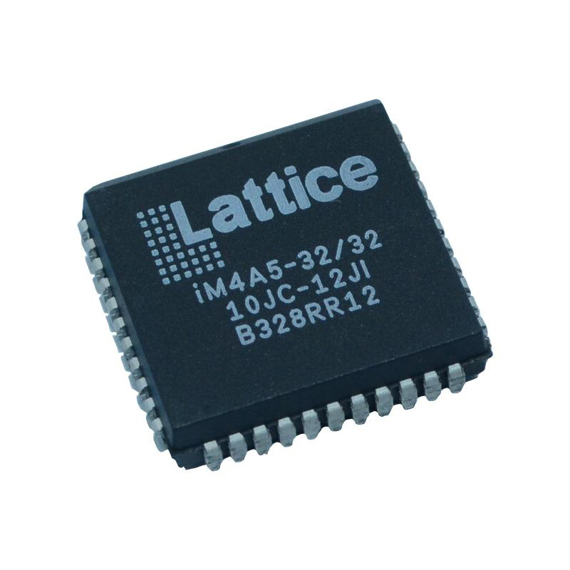

An ultra-low power FPGA and sensor management from Lattice Semiconductor called ICE40UL1K-SWG16ITR is made for ultra-low power mobile applications, including those found in smartphones, tablets, and handheld devices. With the exception of the high-current IR LED driver, the ICE40UL1K-SWG16ITR is compatible with ICE40UL1K-SWG16ITR of devices. The iCE40 UltraPlus also includes an extra 1 Mb SRAM, more DSP blocks, and more LUTs, all of which can be used to offer an always-on voice recognition function in mobile devices without the need to constantly run the more power-hungry voice codec. SPI and I2C blocks that are built into the iCE40 UltraPlus series allow it to interface with almost all mobile sensors and application processors. Two I/O pins of the iCE40 UltraPlus series are also available to support the interface to I3C devices. There are two on-chip oscillators: one is the HFOSC (48 MHz), which can be utilized for wakeup activities, and the other is the LFOSC (10 kHz), which is suited for low power operation in always-on applications. Additionally, the ICE40UL1K-SWG16ITR includes a DSP functional block to off-load the Application Processor's processing of data provided from the mobile device, such as voice data. The ICE40UL1K-SWG16ITR, which has three 24 mA constant current RGB outputs, contains all the circuitry required to drive the service LED directly without the use of an additional MOSFET or buffer. The ICE40UL1K-SWG16ITR is designed to enable mobile apps to carry out all the tasks that can be carried out by ICE40UL1K-SWG16ITR devices, including Service LED, GPIO Expander, SDIO Level Shift, and other specialized features. Additionally, voice recognition applications are targeted for the iCE40 UltraPlus ICE40UL1K-SWG16ITR of devices. Two device densities, 2800 to 5280 Look Up Tables (LUTs) of logic with programmable I/Os that can be utilized as either SPI/I2C interface ports or general purpose I/Os, are available in the ICE40UL1K-SWG16ITR. A higher performance I3C interface can be used with two of the iCE40 UltraPlus I/Os. Additionally, it features 1024 kb of Single Port SRAMs for user logic and up to 120 kb of Block RAMs.
Functional
The architecture of theICE40UL1K-SWG16ITR includes a number of Programmable Logic Blocks (PLB), two Oscillator Generators, two user-configurable I2 C controllers, two user-configurable SPI controllers, blocks of sysMEM Embedded Block RAM (EBR), and Single Port RAM (SPRAM), all encircled by Programmable I/O (PIO). The iCE40UP5K device's block diagram is displayed in Figure 3.1.The SysMEM EBR blocks and Programmable Logic Blocks (PLB) are placed in a two-dimensional grid with rows and columns. There are either PLB or EBR blocks in every column. The PIO cells are stacked in banks and are found at the top and bottom of the device. The foundational elements for logic, arithmetic, and register functions are found in the PLB. A flexible I/O buffer used by the PIOs is known as a sysIO buffer, and it allows for operation with a number of different interface standards. Numerous vertical and horizontal routing channel resources connect the blocks. These routing resources are automatically distributed using the put and route software program. There are three sysIO banks in the ICE40UL1K-SWG16ITR: one on top and two at the bottom. If all the I/Os use the same voltage standard, the user can link a few VCCIOs together. See the section on Power-up Supply Sequence. The sysMEM EBRs are huge, fast memory blocks with a 4 kb size. Using PLBs, these blocks can be set up as RAM, ROM, or FIFO with user logic. The iCE40 UltraPlus devices also have four 256 kb SPRAM blocks that can be cascaded to form up to 1 Mb blocks in addition to the EBR. It is helpful for the short-term storing of massive amounts of data.
| Specification | Value |
|---|---|
| Category | Integrated Circuits (ICs) |
| Mounting Type | Surface Mount |
| Number of I/O | 10 |
| Number of LABs/CLBs | 156 |
| Number of Logic Elements/Cells | 1248 |
| Operating Temperature | -40掳C ~ 100掳C |
| Package / Case | 16-XFBGA, WLCSP |
| Series | UltraLite |
| Standard Package | 5,000 |
| Supplier Device Package | 16-WLCSP (1.4x1.5) |
| Total RAM Bits | 57344 |
| Voltage - Supply | 1.14 V ~ 1.26 V |

Buy ICE40UL1K-CM36AITR1K Lattice Semiconductor, Get familiar with the ICE40UL1K-CM36AITR1K iCE40 Ult...

Buy ICE40UL1K-SWG16ITR50 Lattice Semiconductor, Get familiar with the ICE40UL1K-SWG16ITR50 iCE40 Ult...

Buy ICE40UP5K-B-EVN Lattice Semiconductor, Get familiar with the ICE40UP5K-B-EVN iCE40 UltraPlus Fam...

Buy ICE40UP5K-UWG30ITR50 Lattice Semiconductor, Get familiar with the ICE40UP5K-UWG30ITR50 iCE40 Ult...

Buy ICE40UL640-SWG16ITR50 Lattice Semiconductor, Get familiar with the ICE40UL640-SWG16ITR50 iCE40 U...