A general-purpose power-supply monitor and sequence controller, theISPPAC20-01JIincludes both in-system programmable logic and in-system programmable analog functionalities that are implemented in non-volatile E2 CMOS technology. 10 independent analog input channels are provided by the ISPPAC20-01JI to monitor up to 10 power supply test points. Two independently programmable comparators are available on each of these input channels to provide the high/low and in-bounds/out-of-bounds (window-compare) monitor functionalities. Additionally, four all-purpose digital inputs are available for various control tasks. The ISPPAC20-01JI offers 14 open-drain digital outputs that can be utilized for supervisory and general-purpose logic interface tasks, as well as for regulating DC-DC converters, low-drop-out regulators (LDOs), and optocouplers. It is possible to set up two of these outputs (HVOUT1-HVOUT2) as high-voltage MOSFET drivers. When operating in high-voltage mode, these outputs may deliver up to 8V to drive the gates of n-channel MOSFETs, enabling them to be utilized as high-side power switches that can be programmed to ramp up and ramp down at different rates. The ISPPAC20-01JI includes a 24-macrocell CPLD that may be utilized to carry out combinatorial logic operations as well as complicated state machine sequencing for the control of several power supplies. The CPLD array uses the condition of each comparator on each analog input channel as well as the general-purpose digital inputs as inputs, and the CPLD may control any digital output. From 32 milliseconds to two seconds can be added to delays and time-outs via four separately programmable timers. LogiBuilder, a simple-to-learn language built into the PAC-Designer software, is used to program the CPLD. To keep track of the condition of any analog input channel comparators or digital inputs, control sequences are written.The ISPPAC20-01JI's I2 C bus or JTAG interface is utilized to monitor the VMON voltage using the on-chip 10-bit A/D converter. The I2 C bus/SMBus interface enables an external microcontroller to operate logic signals IN2 to IN4 and output pins, read back the status of each VMON comparator and PLD output, and measure the voltages attached to the VMON inputs (ISPPAC20-01JIonly). All I2 C registers can be read out during manufacture via the JTAG interface.
| Specification | Value |
|---|---|
| Logic Family | ISPPA |
| Delay Time | 5 ns |
| Operating Supply Voltage | 3 V to 3.6 V |
| Maximum Operating Temperature | + 85℃ |
| Minimum Operating Temperature | - 40℃ |
| Mounting Style | SMD/SMT |
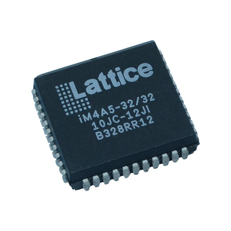
| Package / Case | PLCC-44 |
| Operating Temperature | - 40℃ to + 85℃ |
| Factory Pack Quantity | 26 |
Buy ISPPAC20-01TI Lattice Semiconductor, Get familiar with the ISPPAC20-01TI ISPPAC Family at VEKEMO...
Buy ISPPAC20-01JI Lattice Semiconductor, Get familiar with the ISPPAC20-01JI ISPPAC Family at VEKEMO...
Buy ISPPAC10-01PI Lattice Semiconductor, Get familiar with the ISPPAC10-01PI ISPPAC Family at VEKEMO...
Buy ISPPAC10-01SI Lattice Semiconductor, Get familiar with the ISPPAC10-01SI ISPPAC Family at VEKEMO...
Buy ISPPAC30-01SI Lattice Semiconductor, Get familiar with the ISPPAC30-01SI ISPPAC Family at VEKEMO...