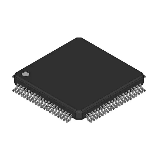
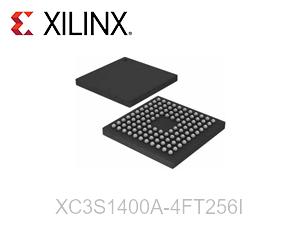
XC3S400A-4FTG256C Description
The XC3S400A-4FTG256C is a member of the Spartan-3A family of Field Programmable Gate Arrays (FPGAs) produced by Xilinx. This device is renowned for its versatility and efficiency in implementing complex digital designs. The Spartan-3A series is specifically engineered for cost-sensitive applications, making the XC3S400A an excellent choice for a wide range of markets, from consumer electronics to industrial automation.
Functionality
The primary function of the XC3S400A-4FTG256C is to provide a platform for digital logic design that can be reconfigured even after manufacturing. This capability enables engineers to prototype and deploy designs rapidly, ensuring that products can adapt to evolving requirements. The FPGA's programmable architecture allows for a diverse range of applications, including signal processing, data routing, and custom hardware implementation.
Technical Specifications
The XC3S400A-4FTG256C features:
- Logic Cells: 400, providing substantial logic resources for implementing complex algorithms.
- I/O Pins: 256, allowing for a high degree of connectivity.
- Maximum Clock Frequency: Up to 200 MHz, supporting high-speed operations.
- Configurable Memory: Contains Block RAM resources for data storage and buffering.
- Power Supply Voltage: Operates at 1.2V core voltage, optimizing power consumption.
- Temperature Range: Designed for industrial applications with an extended temperature range of -40°C to +100°C.
- Package Type: Available in a Fine Pitch Ball Grid Array (FBGA) package for efficient thermal and electrical performance.
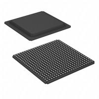
XC3S400A-4FTG256C Pinout Diagram
Pinout Overview
The XC3S400A-4FTG256C includes various pins for power, ground, configuration, and I/O operations. Each pin is designed with specific electrical characteristics to ensure optimal performance.
- VCCINT: Power supply for the internal logic (1.2V).
- VCCIO: Power supply for I/O banks; can be configured for different voltage levels.
- GND: Ground connections that help stabilize the device.
- I/O Pins: Configurable as input, output, or bidirectional, with characteristics like TTL compatibility and programmable drive strength.
- JTAG Pins: For configuration and debugging.
Electrical Characteristics
Each I/O pin can be programmed for various standards such as LVTTL, LVCMOS, and more, providing flexibility in interfacing with other devices. Maximum current ratings and input/output thresholds are defined to maintain integrity and reliability across different application scenarios.
XC3S400A-4FTG256C Features
- Reprogrammability: The XC3S400A can be reconfigured multiple times, making it ideal for prototyping and iterative design processes.
- High Performance: Capable of running at high clock frequencies, it ensures that time-critical applications can be addressed effectively.
- Low Power Consumption: The advanced manufacturing process and design techniques lead to reduced power consumption, critical for battery-operated devices.
- Integrated DSP Blocks: Facilitates efficient signal processing capabilities, enhancing performance in communications and audio processing applications.
- Rich I/O Support: Supports various I/O standards and configurations, allowing seamless integration with other digital components.
XC3S400A-4FTG256C Applications
The versatility of the XC3S400A-4FTG256C makes it suitable for numerous application scenarios:
- Consumer Electronics: Used in devices such as digital cameras, video game consoles, and set-top boxes, where customization and rapid development are essential.
- Industrial Automation: Employed in control systems and data acquisition, allowing manufacturers to create tailored solutions that enhance operational efficiency.
- Telecommunications: Facilitates protocol bridging, signal processing, and network interface functions in communication devices, ensuring robust data transfer.
- Medical Devices: Utilized in diagnostic and monitoring equipment, enabling real-time data processing and analysis.
XC3S400A-4FTG256C Alternative Models
Several alternative models offer similar capabilities:
- XC3S200A: A smaller version with fewer logic cells, suitable for simpler applications.
- XC3S1000: Provides more logic resources and I/O pins, ideal for more complex designs.
- Lattice iCE40: A competitive low-power FPGA option with similar performance characteristics but different architectural advantages.
Frequently Asked Questions about XC3S400A-4FTG256C
How do I install the XC3S400A?
- Installation typically requires an appropriate development board and a JTAG programmer for configuration.
Is the XC3S400A compatible with other Xilinx products?
- Yes, it is designed to work seamlessly within the Xilinx ecosystem, including tools like Vivado and ISE.
What are the best practices for optimizing performance?
- Use the dedicated DSP blocks for signal processing tasks and minimize unnecessary logic to enhance speed.
How do I troubleshoot configuration issues?
- Check the JTAG connections and ensure the correct voltage levels are supplied to the device.
Technical Specifications
- Logic Cells: 400
- I/O Pins: 256
- Max Clock Frequency: 200 MHz
- Power Supply Voltage: 1.2V (core), configurable for I/O
- Temperature Range: -40°C to +100°C
- Package Type: FBGA
References
- Xilinx Product Documentation
- FPGA Development Kit User Guides
- Application Notes on Spartan-3A series
XC3S400A-4FTG256C Specifications
| Specification | Value |
|---|
| Number of LABs/CLBs | 896 |
| Number of Logic Elements/Cells | 8064 |
| Total RAM Bits | 368640 |
| Number of I/O | 195 |
| Number of Gates | 400000 |
| Voltage - Supply | 1.14V ~ 1.26V |
| Mounting Type | Surface Mount |
| Operating Temperature | 0℃ ~ 85℃ (TJ) |
| Package / Case | 256-LBGA |
| Supplier Device Package | 256-FTBGA (17x17) |
Application Field
-

Artificial Intelligence
-

5G Technology
-

Cloud Computing
-

Consumer Electronics
-

Wireless Technology
-

Industrial Control
-

Internet of Things
-

Medical Equipment