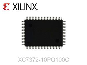
The XC7372-10PQ100C comes in pin-grid array (PGA), ball-grid array (BGA), and quad flat pack (QFP) packaging, as well as plastic and ceramic leaded chip carriers. Windowed ceramic packaging for design prototypes and one-time programmable plastic packaging for high production volumes are available as alternatives. The XC7372-10PQ100C Devices have a special Dual-Block design that allows for high density capability via High Density Function Blocks and/or high speed operations via Fast Function Blocks. For crucial decoding and ultrafast state machine applications, Fast Function Blocks (FFBs) offer fast, pin-to-pin speed and logic throughput. For adders, accumulators, wide functions, state machines needing a large number of product terms, and other types of complicated logic, High-Density Function Blocks (FBs) offer the maximum logic density and system-level functionality to construct complex functions with predictable time. The Universal Interconnect Matrix (UIM), which ensures 100% interconnectivity of all internal processes, is also utilized by the XC7372-10PQ100C architecture. For any routing path across the UIM, this interconnect architecture offers consistent, brief connectivity delays. Constant connectivity delays, independent of logic arrangement within the chip, simplify device timing and ensure design performance. View Substitutes & Alternatives, datasheets, stock, pricing from Authorized Distributors, as well as other FPGAs goods, at www.vemeko.com.
DSP slices with an optimized symmetric coefficient filter and a 25 x 18 multiplier, 48-bit accumulator, and pre-adder for high-performance filtering.
Phase-locked loop (PLL) and mixed-mode clock manager (MMCM) blocks are combined in powerful clock management tiles (CMT) for high precision and low jitter.
Utilize the MicroBlazeTM processor to quickly install embedded processing.
PCI Express® (PCIe) integrated block supports up to x8 Gen3 Endpoint and Root Port designs.
Numerous configuration options, including HMAC/SHA-256 authentication, built-in SEU detection and correction, and support for common memory types.
Flip-chip packaging that is low-cost, wire-bonded, bare-die, and high signal integrity and allows for simple family migration in the same package. Both Pb-free versions of all packages and Pb versions of some packages are offered.
With 28 nm, HKMG, HPL process, 1.0V core voltage process technology, and 0.9V core voltage option for even lower power, it is designed for maximum performance and lowest power.
High-speed arithmetic carry network with 18-bit accumulators operating at 43 to 61 MHz and a 1 ns ripple-carry latency per bit
Several separate clocks
Every input can be set to be registered, latched, or direct.
24 mA high-drive output with 3.3 V or 5 V I/O operation
3.3 V ±0.3 V JEDEC Standard (8-1A) is met.
Options for power control
Several security components to safeguard designs
Equipped with design and verification tools that are industry standard
| Specification | Value |
|---|---|
| Typical 22V10 Equivalent | 8 |
| Number of Macrocells | 72 |
| Number of Function Blocks | 8 |
| Number of Flip-Flops | 126 |
| Number of Fast Inputs | 12 |
| Number of Signal Pins | 84 |

Buy XC73108-10PQ160C Xilinx, Inc, Get familiar with the XC73108-10PQ160C XC7300 CMOS EPLD at VEKEMO ...
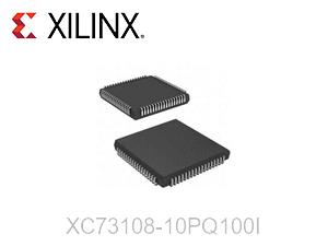
Buy XC73108-10PQ100I Xilinx, Inc, Get familiar with the XC73108-10PQ100I XC7300 CMOS EPLD at VEKEMO ...
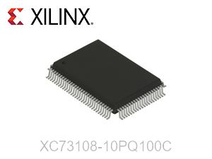
Buy XC73108-10PQ100C Xilinx, Inc, Get familiar with the XC73108-10PQ100C XC7300 CMOS EPLD at VEKEMO ...
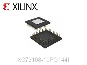
Buy XC73108-10PG144I Xilinx, Inc, Get familiar with the XC73108-10PG144I XC7300 CMOS EPLD at VEKEMO ...

Buy XC73108-10PG144C Xilinx, Inc, Get familiar with the XC73108-10PG144C XC7300 CMOS EPLD at VEKEMO ...