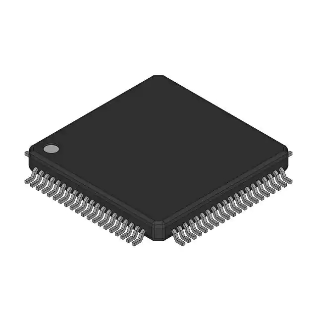
Programmable configuration within the system In XCF01SVOG20C, PROMs from Xilinx are now accessible. The FPGA generates a configuration clock when it is in Master Serial mode, which is used to drive the PROM. After a brief access time following the activation of CE and OE, data is accessible on the PROM DATA (D0) pin, which is coupled to the FPGA DIN pin. Fresh data becomes temporarily available after each rising clock edge. The FPGA generates the appropriate number of clock pulses to complete the configuration. The PROM and the FPGA are clocked by an external clock when the FPGA is operating in slave serial mode. When in Master SelectMAP mode, the XCF01SVOG20C generates a configuration clock that drives the PROM mode.
• In-System Programmable PROMs for Configuration of Xilinx® FPGAs
• Low-Power Advanced CMOS NOR Flash Process
• Endurance of 20,000 Program/Erase Cycles
• JTAG Command Initiation of Standard FPGA Configuration
• Cascadable for Storing Longer or Multiple Bitstreams
• IP and Smart camera
• Video and night vision equipment
• LTE radio and baseband
• Multifunction printers
| Specification | Value |
|---|---|
| Supply Voltage (DC) | 3.30 V, 3.60 V (max) |
| Clock Speed | 50.0 MHz |
| Memory Size | 125000 B |
| Product Lifecycle Status | Active |
| Packaging | Tube |
| Mounting Style | Surface Mount |
| Number of Pins | 20 |
| Case/Package | TSSOP |
| RoHS | Compliant |
| Lead-Free Status | Lead Free |
| REACH SVHC Compliance | No SVHC |
| HK STC License | NLR |
Buy XC18V02VQ44I Xilinx, Inc, Get familiar with the XC18V02VQ44I Memory - Configuration Proms for FP...
Buy XC17128ELPD8I Xilinx, Inc, Get familiar with the XC17128ELPD8I Memory - Configuration Proms for ...
Buy XC17128ELPD8C Xilinx, Inc, Get familiar with the XC17128ELPD8C Memory - Configuration Proms for ...
Buy XC17128ELPC20I Xilinx, Inc, Get familiar with the XC17128ELPC20I Memory - Configuration Proms fo...
Buy XC17128ELPC20C Xilinx, Inc, Get familiar with the XC17128ELPC20C Memory - Configuration Proms fo...