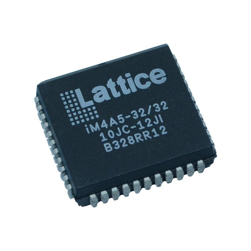
Both 3.3V and 5V signal levels can be interfaced with by the GAL16LV8C. The GAL16LV8-15LJN is created utilizing the cutting-edge 3.3V E2 CMOS process from Lattice Semiconductor, which combines CMOS and Electrically Erasable (E2) floating gate technology. The devices can be reprogrammed rapidly and effectively thanks to high speed erase times (100ms).
The 3.3V GAL16LV8-15LJN has the same 16V8 architecture as its 5V equivalent, which is the industry standard, and it is capable of supporting all architectural features including combinatorial or registered macrocell operations.
Complete AC, DC, and functional testing may be done while manufacturing thanks to special test circuitry and reprogrammable cells. Because of this, Lattice Semiconductor provides all GAL products with 100% field programmability and functionality. Furthermore requested are 100 erase/write cycles and data retention periods longer than 20 years.
